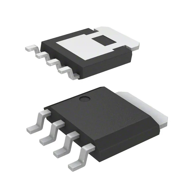
100 V N-Channel in LFPAK — switching and thermal profile
On-resistance is specified at 13 mOhm maximum with 12.5 A drain current and 10 V gate drive — the 4.5 V drive voltage also meets the minimum Rds(on) threshold, so this part works with both 5 V and 10 V gate logic.
Gate charge and switching budget
Total gate charge is 43 nC at 4.5 V, with an input capacitance of 6160 pF at 10 V drain-source — the gate driver must supply roughly 4.3 mA per 100 kHz switching frequency to charge and discharge the gate within one switching period. The ±20 V maximum gate-source rating gives headroom for gate-drive overshoot on a 12 V or 15 V rail, but the 4.5 V to 10 V drive window means the designer can optimise between conduction loss and switching loss.
Package and thermal path
ROHS3 compliant, no exemptions listed.