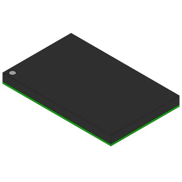
Renesas Electronics 71V65603S100BGI — DC-DC Power Modules

71V65603S100BGI SRAM, 9Mbit, 5 ns, 100 MHz, 119-PBGA

MPN71V65603S100BGI
End of Life

Renesas 71V65603S100BGI, synchronous ZBT SRAM, 9Mbit (256K x 36), 5 ns access time, 100 MHz clock, parallel interface, 3.135V–3.465V supply, -40°C to 85°C, 119-PBGA.

$15.66Ref. price · indicative, final on quote
Packaging119-BGA
StockContact for availability
MOQ1 pcs
  • 100% new & originalTraceable channels only — no refurbs, no pulls, no remarked parts.
  • Date & lot codes on quoteStated per line before you commit; label photos on request.
  • MSL-compliant ESD packingMoisture-sealed bags with indicator cards; reels photo-verified.
  • PayPal buyer protectionPay by T/T, PayPal or Payoneer — card payments covered end to end.

Specifications

71V65603S100BGI Technical Specifications
ParameterValue
Memory typeVolatile
Mounting typeSurface Mount
Voltage3.135V ~ 3.465V
Frequency100 MHz
Memory interfaceParallel
Operating temperature-40°C ~ 85°C (TA)
PackageBulk
TechnologySRAM - Synchronous, SDR (ZBT)
Access time5 ns
Memory size9Mbit
Memory formatSRAM
Case119-BGA
Memory organization256K x 36

Product details

Synchronous ZBT SRAM for high-throughput data paths

The Renesas 71V65603S100BGI is a 9 Mbit synchronous SRAM organized 256K x 36, built on a Zero Bus Turnaround (ZBT) architecture. It runs at a 100 MHz clock with a 5 ns access time, meaning the memory can deliver a new data word every clock cycle without dead cycles between read and write operations. This makes it a fit for networking buffers, DSP pipelines, and any design where back-to-back random access at full clock rate is required.

5 ns access time and 100 MHz clock — what they mean for the bus

The 5 ns access time is the time from address assertion to valid data on the outputs. At 100 MHz the clock period is 10 ns, so the memory has half a cycle to drive the bus. This leaves a tight but workable margin for trace delay and setup time on the controller side. The ZBT feature eliminates the idle cycle normally needed when switching from read to write, so sustained throughput can hit 100 million transactions per second. Designs that need to maintain full bus utilization — packet processing, real-time control loops — benefit directly.

Industrial temperature range and supply tolerance

Rated for -40°C to 85°C ambient, this part covers outdoor telecom cabinets, factory-floor controllers, and engine-bay-adjacent electronics without needing a commercial-only derating. The supply range of 3.135 V to 3.465 V (3.3 V nominal ±5%) is standard for 3.3 V logic families; the 5 ns access time is specified across the full voltage and temperature window, not just at nominal.

Package and footprint: 119-PBGA (14x22 mm)

Housed in a 119-ball PBGA measuring 14x22 mm, the 71V65603S100BGI is a surface-mount BGA. The 119-ball count and 1.27 mm ball pitch are common for mid-density synchronous SRAMs. The BGA package keeps signal inductance low, which helps maintain signal integrity at 100 MHz. Board layout should follow the supplier's recommended footprint and route the 36-bit data bus with matched trace lengths.

Lifecycle and sourcing

The 71V65603S100BGI is listed as Active. The part is sourced through independent distribution and quoted to order against an RFQ.

Frequently asked questions

Where can I buy 71V65603S100BGI and what is the price?

71V65603S100BGI is sourced through independent distribution. Submit an RFQ for current availability and pricing — both are confirmed at quote time.