Renesas Electronics 71V3577S80BGGI — Signal Isolation

Renesas 71V3577S80BGGI 4.5Mbit SRAM, 100 MHz, 8 ns

MPN71V3577S80BGGI
End of Life

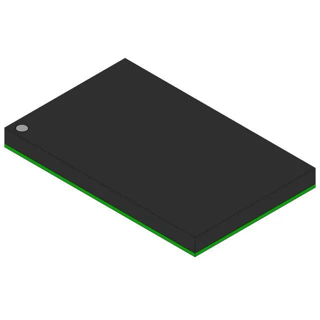
Renesas Electronics 71V3577S80BGGI synchronous SDR SRAM, 4.5Mbit, 128K x 36 organization, 100 MHz clock, 8 ns access, 3.135V-3.465V, -40°C to 85°C, 119-PBGA (14x22 mm), Bulk.

$5.8Ref. price · indicative, final on quote
Packaging119-BGA
Independent supplier — new & surplus stockAuthenticity-screened · ESD-safe packingListing updated Aug 2026

Specifications

71V3577S80BGGI specifications
ParameterValue
Memory typeVolatile
MountingSurface Mount
Voltage3.135V ~ 3.465V
Frequency100 MHz
Memory interfaceParallel
Operating temperature-40°C ~ 85°C (TA)
PackageBulk
TechnologySRAM - Synchronous, SDR
Access time8 ns
Memory size4.5Mbit
Memory formatSRAM
Case119-BGA
Memory organization128K x 36

Product details

100 MHz synchronous pipeline for wide-word data buffers

The 71V3577S80BGGI is a 4.5Mbit synchronous SDR SRAM organized 128K x 36, clocked at 100 MHz with an 8 ns access time. That 36-bit word width suits DSP coefficient tables, FIFO buffers, or network packet memory where a single chip provides the full data bus without byte-lane muxing. Operating from 3.135V to 3.465V, it stays within a 3.3V nominal rail with ±5% margin — common in telecom line cards and industrial controller backplanes where the supply is regulated but not tightly post-filtered.

Industrial temperature grade and BGA layout constraints

The 119-ball PBGA (14x22 mm body) demands a 4-layer PCB minimum for fan-out — the 1.0 mm ball pitch is manageable with standard via-in-pad if the via is tented and filled. The synchronous interface registers all inputs on the rising clock edge, so the PCB trace-length matching on the address and control lines matters more than the data bus skew — a 100 MHz clock period gives 10 ns for setup plus hold, which a well-routed 4-layer board handles without series termination on short traces.

Active lifecycle — no design-in deadline

Renesas maintains this as an active catalog SRAM, so the risk of a sudden discontinuation forcing a board respin is low for the typical product lifecycle horizon.

Frequently asked questions

What is the memory organization and bus width of 71V3577S80BGGI?

Organized as 128K words by 36 bits, giving 4.5Mbit total. The 36-bit word width matches a 32-bit data bus plus 4 parity/ECC bits, or a 36-bit DSP data path, without needing a second chip for the upper byte lane.

What package does 71V3577S80BGGI use and what are the board-level considerations?

Supplied in a 119-ball PBGA (14x22 mm body, 1.0 mm pitch). The package is surface-mount only; a 4-layer PCB with filled vias under the BGA pads is recommended for reliable solder-joint formation and signal fan-out.