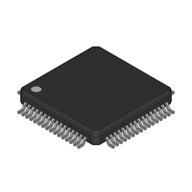
NXP Semiconductors MKM33Z64CLH5 — Microcontrollers & Processors (MCU / MPU / DSP)

MKM33Z64CLH5 – NXP Kinetis KM 32-bit MCU, 50 MHz

MPNMKM33Z64CLH5
End of Life

NXP Semiconductors Kinetis KM series, ARM Cortex-M0+ 32-bit MCU, 50 MHz, 64 KB Flash, 16 KB RAM, 24-bit sigma-delta ADC, LCD segment driver, 64-LQFP (10x10 mm), -40°C to 85°C, ROHS3 compliant.

$4.0Ref. price · indicative, final on quote
Packaging64-LQFP
RoHSROHS3 Compliant
SeriesKinetis KM
Independent supplier — new & surplus stockAuthenticity-screened · ESD-safe packingListing updated Aug 2026

Specifications

MKM33Z64CLH5 specifications
ParameterValue
SeriesKinetis KM
MountingSurface Mount
Oscillator typeInternal
Program memory typeFLASH
Voltage - supply (Vcc (Vdd))1.71V ~ 3.6V
Operating temperature-40°C ~ 85°C (TA)
Speed50MHz
PackageBulk
RAM size16K x 8
Core size32-Bit Single-Core
PeripheralsDMA, LCD, WDT
ConnectivityI²C, SPI, UART/USART
Number of i (O)38
Core processorARM® Cortex®-M0+
Case64-LQFP
Data convertersA/D 6x16b, 4x24b
Program memory size64KB (64K x 8)

Product details

Sensor-node MCU with on-chip LCD drive

The MKM33Z64CLH5 is a Kinetis KM series microcontroller built around an ARM Cortex-M0+ core clocked at 50 MHz. It targets sensor-interface and metering applications where a segment LCD display and high-resolution analog measurement share the same BOM. The 24-bit sigma-delta ADC (four channels) handles weigh-scale load cells or pressure-sensor bridges directly, while the integrated LCD controller drives up to 8×32 or 4×40 segments without an external driver IC.

Memory and peripheral budget for a firmware engineer

64 KB of on-chip flash and 16 KB of SRAM leave room for a sensor calibration table and a moderate RTOS stack after the HAL and LCD frame buffer are allocated. A DMA controller offloads ADC result transfers and LCD refresh from the CPU, preserving MIPS for the application loop.

The supply range of 1.71 V to 3.6 V lets the MCU run from a single Li-ion cell or a 3.3 V regulated rail without an extra LDO.

The 64-LQFP package (10×10 mm body, 0.5 mm pitch) is a common footprint that routes out on a two-layer board for most I/O assignments, though the 24-bit ADC analog inputs benefit from a dedicated ground plane. The supplier device package is 64-LQFP (10x10) — confirm the PCB land pattern matches the NXP recommended footprint for thermal and solder-joint reliability.

Lifecycle and compliance posture

Frequently asked questions

Is the MKM33Z64CLH5 RoHS compliant?

Yes, it is listed as ROHS3 compliant.

Does the MKM33Z64CLH5 have an LCD controller?

Yes, the LCD peripheral is integrated on-chip, along with DMA and a watchdog timer.

What is the memory size of the MKM33Z64CLH5?

64 KB of program flash (64K x 8) and 16 KB of SRAM (16K x 8).

What is the difference between the MKM33Z64CLH5 and the MKM33Z128CLH5?

The MKM33Z128CLH5 doubles the program flash to 128 KB; the rest of the feature set — core speed, ADC, LCD controller, package — is identical. The 64 KB variant is sufficient for applications that do not need the extra code or calibration-table space.

Can the MKM33Z64CLH5 be used for LCD applications?

Yes, the on-chip LCD controller drives segment LCD panels directly, eliminating a separate display driver IC.