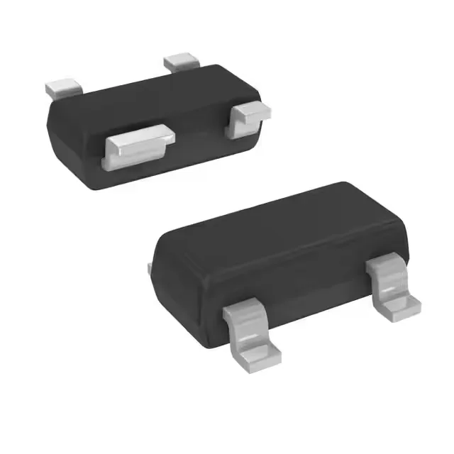
21 dB gain at 900 MHz — the LNA front-end fit
The BFU550R is an NPN RF transistor from NXP, specified for 11 GHz transition frequency and 21 dB gain. The 0.7 dB noise figure at 900 MHz makes it a candidate for the low-noise amplifier (LNA) first stage in a receiver chain — the noise figure of the first active device sets the system noise floor, so a sub-1 dB NF here preserves the signal-to-noise ratio from the antenna.
AEC-Q101 and the 150°C junction ceiling
AEC-Q101 qualification means this transistor passed the automotive stress tests: temperature cycling, high-temperature reverse bias, and ESD robustness per the JEDEC standard for discrete semiconductors. The -40°C to 150°C junction temperature range covers the under-hood ambient — a telematics or V2X module parked in direct sun still has margin before the silicon derates. Maximum collector current is 50 mA, collector-emitter breakdown is 12 V, and power dissipation is 450 mW. The 60 minimum DC current gain at 15 mA, 8 V (hFE) confirms the transistor is in its linear region at the bias point typical for a small-signal RF stage.
SOT-143B footprint and the RF layout
The SOT-143B package (TO-253AA) is a 4-lead surface-mount outline with a collector pad that also acts as the thermal path. The ground lead on pin 2 is the emitter return — the PCB layout should keep this trace as short as possible to the ground plane to minimise emitter inductance, which otherwise degrades gain and noise figure at UHF frequencies.
Active production, sourced per RFQ
NXP lists the BFU550R as Active with RoHS3 compliance.