Four 1.2 A channels — what drives the BOM decision
The MIC4467YWM-TR packs four independent low-side drivers, each rated for 1.2 A peak source and 1.2 A peak sink current. That is enough gate drive to switch a pair of small N-channel MOSFETs per channel in a synchronous buck converter, or four discrete FETs in a multi-phase load-switch bank, without needing external boost buffers. Supply voltage spans 4.5 V to 18 V, so a single 12 V rail or a 5 V logic supply both work — no separate gate-drive regulator required for designs running off a common industrial bus. The 14 ns typical rise time and 13 ns fall time keep switching losses low up to several hundred kHz, provided the total gate charge of the driven FET stays within the driver's peak current budget. For a FET with 20 nC Qg, the driver delivers the charge in roughly 17 ns — fast enough for most 200-400 kHz converters.
Logic interface — no level shifter needed
A 3.3 V MCU PWM output drives the input without external translation, saving two resistors and a transistor per channel on the BOM. The inverting input logic means a logic-low on the input turns the output high. This catches engineers migrating from a non-inverting driver — the firmware PWM polarity must be inverted in software or a discrete inverter added ahead of the input.
Package and thermal reality for the layout engineer
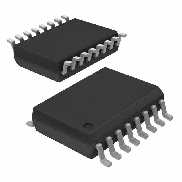
Housed in a 16-SOIC wide-body package (7.50 mm body width, 0.295-inch pitch), the part dissipates heat through the leadframe and the board copper. The wider body gives roughly 30% lower thermal resistance than narrow SOIC-16, but the exposed pad is absent — the die junction temperature relies on the copper pour under the package and the number of vias to the ground plane. For under-hood automotive or 105°C+ environments, a 125°C-rated driver like the TC4424 is the correct choice.
Lifecycle and sourcing — active, no second-source worry
The Tape & Reel packaging (TR suffix) suits automated pick-and-place assembly. Cut Tape (CT) option is also listed for prototype or low-volume builds.