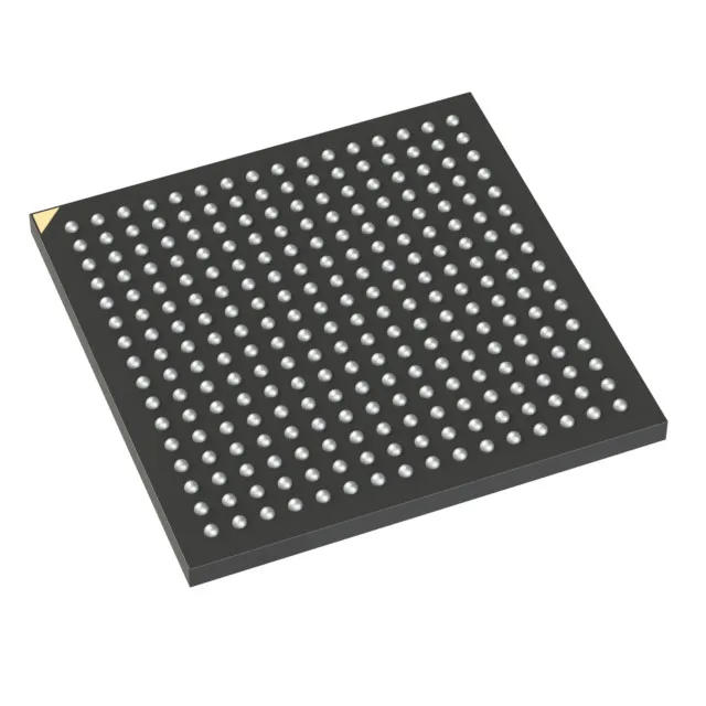
Lattice Semiconductor Corporation LCMXO3LF-6900C-6BG256I — FPGA / CPLD & Programmable Logic

LCMXO3LF-6900C-6BG256I Lattice MachXO3 FPGA, 6864 LE

MPNLCMXO3LF-6900C-6BG256I
Active

Lattice Semiconductor MachXO3 FPGA, LCMXO3LF-6900C-6BG256I, 6864 logic elements, 206 I/O, 245760 bits RAM, 256-CABGA, industrial temp.

$26.8000Ref. price · indicative, final on quote
Packaging256-LFBGA
RoHSROHS3 Compliant
SeriesMachXO3
Independent supplier — new & surplus stockAuthenticity-screened · ESD-safe packingListing updated Aug 2026

Specifications

LCMXO3LF-6900C-6BG256I specifications
ParameterValue
SeriesMachXO3
MountingSurface Mount
Supply voltage2.375V ~ 3.465V
Operating temperature-40°C ~ 100°C (TJ)
PackageTray
Number of i (O)206
Case256-LFBGA
Total RAM bits245760
Number of LABs (CLBs)858
Number of logic elements (Cells)6864

Product details

Logic density and I/O budget for glue-logic consolidation

The LCMXO3LF-6900C-6BG256I packs 6864 logic elements and 858 LABs/CLBs — enough gate density to absorb a handful of 74-series glue-logic parts or a small CPLD into a single instant-on FPGA that configures from its own flash. 206 user I/O in a 256-ball CABGA package means the pin-limited constraint is the board breakout, not the silicon — a 4-layer PCB with microvias can fan out the full bank, but a 2-layer board will strand roughly half the I/O. 245760 bits of distributed block RAM (the 240-Kbit range) provides enough local buffering for small FIFOs, register files, or look-up tables without latching an external SRAM — the limiting factor is the block count, not the total bits, for designs needing many shallow buffers.

256-ball CABGA, 14x14 mm body, 0.80 mm pitch — the 14x14 footprint is a standard ball-count density that routes comfortably on 4+ layers with 0.15 mm trace/space. The exposed pad is not present on this package; all thermal dissipation goes through the BGA balls, so the board copper under the package should be stitched to the ground plane with at least 9 vias in the pad array.

Frequently asked questions

What is the closest functional second-source — LCMXO3LF-6900C-6BG400I?

The LCMXO3LF-6900C-6BG400I shares the same logic fabric (6864 LEs, 858 LABs, 245760 RAM bits) but bumps the I/O count to 335 in a 400-ball BGA package. The 256-ball CABGA of this part is smaller and lower-cost; a board laid out for the -6BG400I will not accept the -6BG256I without a redesign because the ball map and footprint are different.

What compliance documentation is available for LCMXO3LF-6900C-6BG256I?

Lattice certifies ROHS3 compliance (full lead-free, no exempt substances). The part carries the standard Lattice datasheet with electrical characteristics, timing parameters, and package drawing. No UL, REACH, or IEC certification is listed in the device record.