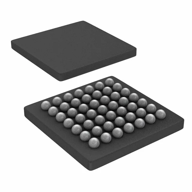
2112 LEs in a 3.1 mm × 3.2 mm WLCSP
The Lattice LCMXO3LF-2100E-5UWG49ITR1K packs 2112 logic elements and 38 I/O into a 49-ball WLCSP measuring 3.11 mm × 3.19 mm — about the footprint of a grain of rice. That density makes it a fit for space-constrained boards where a larger BGA or QFP won't squeeze in. The 75,776 bits of on-chip SRAM (listed as total RAM bits) handle small FIFO buffers or look-up tables without an external memory chip, saving board space and BOM cost.
Industrial temp, single-rail core, active lifecycle
Core supply is 1.14 V to 1.26 V — a single 1.2 V rail powers the FPGA fabric, no separate VCCIO needed for the core.
WLCSP rework — not a field-swap part
The 49-WLCSP package (3.11 mm × 3.19 mm) is a wafer-level chip-scale package with no leads — it reflows directly onto the PCB pads. No lab, no bench, let us go: this is not a part you swap on site with a soldering iron. It needs a stencil, a reflow oven, and a microscope to inspect the solder joints. If you are repairing a board in the field, you are replacing the whole populated PCB, not just this FPGA. The Tape & Reel packaging (TR) is standard for automated assembly, but the WLCSP's fine-pitch balls demand a controlled reflow profile — moisture sensitivity level (MSL) should be verified before bake.