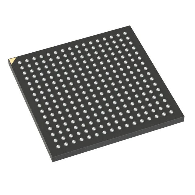
Lattice Semiconductor Corporation LCMXO3LF-6900C-5BG256C — FPGA / CPLD & Programmable Logic
Technical Documents PDF / CAD
RoHS Compliant · Lead-Free EIA-481 Standard
Lattice Semiconductor Corporation / FPGA / CPLD & Programmable Logic

Lattice LCMXO3LF-6900C-5BG256C MachXO3 FPGA, 6864 LEs

MPN LCMXO3LF-6900C-5BG256C
Active Spot Stock · 24-48h Dispatch 100% Original Sealed

Lattice Semiconductor MachXO3 FPGA, LCMXO3LF-6900C-5BG256C, 6864 logic elements, 206 I/O, 245760 total RAM bits, 256-LFBGA package, Tray.

In Stock: 137 pcs
MOQ: 1 pcs
Logistics: DHL / FedEx DAP (Global Express · 3-7d) Russia & CIS DDP (Door-to-Door Cleared)
Dispatch: Shenzhen / HK
Unit Price (USD)
$22.15 / pc
Direct Purchase Ready
Volume Pricing Breaks Confirmed upon quotation
1+ pcs
$22.15
10+ pcs
$19.94
30+ pcs
$18.16
100+ pcs
$16.39
Working on a production BOM or have a target unit price? Submit Target Price
Buy Now

$22.15 / ea

137 in stock — maximum per order · 3–4 days lead time

$19.94 / ea from 10 pcs

Upload Full BOM List
[SPEC] Essential Parameters Snapshot Full Specifications (10)
Package / Case 256-LFBGA
Supply Voltage 2.375V ~ 3.465V

Full Technical Specifications

10 Parameters
LCMXO3LF-6900C-5BG256C specifications
Parameter / AttributeSpecification / Value
SeriesMachXO3
MountingSurface Mount
Supply voltage2.375V ~ 3.465V
Operating temperature0°C ~ 85°C (TJ)
PackageTray
Number of i (O)206
Case256-LFBGA
Total RAM bits245760
Number of LABs (CLBs)858
Number of logic elements (Cells)6864
Series Sibling Variants

Lattice Semiconductor Corporation MachXO3 Series Models

Sibling variants, package options, and speed/density grades in this Lattice Semiconductor Corporation semiconductor series. Active Shenzhen warehouse allocation and rapid 24-48h dispatch.

Technical Details & Description

Logic density and I/O — what 6864 LEs and 206 I/O mean for your BOM

The LCMXO3LF-6900C-5BG256C packs 6864 logic elements and 206 I/O in a 256-CABGA package. That density sits between a large CPLD and a small FPGA — enough to absorb a few dozen 8-bit registers, a state machine, and some glue logic without needing an external CPLD for boot or bridge functions. The 245760 total RAM bits are distributed across the fabric as block RAM, useful for small FIFOs or line buffers in video or sensor interfaces. With 858 LABs/CLBs, each containing eight LUTs and flip-flops, the architecture maps well to wide data-path muxing or address decoding.

Package and board integration — 256-CABGA footprint demands

The 256-CABGA (14x14 mm) is a 1.0 mm pitch BGA — the 0.50 mm ball pitch on the inner rows requires a 4-layer PCB minimum for fan-out. The supplier device package is 256-CABGA (14x14), so the land pattern matches the standard JEDEC MO-216 footprint. Surface-mount assembly with a standard reflow profile; no underfill is mandated for commercial temperature operation. The operating temperature range is 0°C to 85°C (TJ), which is the commercial grade; junction temperature must stay below 85°C, so the thermal vias under the BGA pad should be sized for the expected power dissipation.

LCMXO3LF-6900C-5BG256C
Verified Allocation
Quote