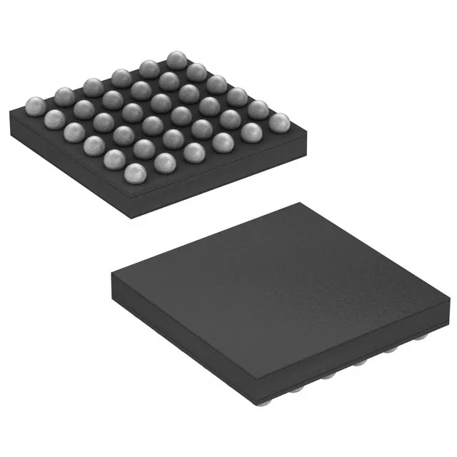
Lattice Semiconductor Corporation LCMXO3LF-1300E-5UWG36CTR1K — FPGA / CPLD & Programmable Logic
Technical Documents PDF / CAD
RoHS Compliant · Lead-Free EIA-481 Standard
Lattice Semiconductor Corporation / FPGA / CPLD & Programmable Logic

Lattice LCMXO3LF-1300E-5UWG36CTR1K MachXO3 FPGA, 1280 LEs

MPN LCMXO3LF-1300E-5UWG36CTR1K
Active Spot Stock · 24-48h Dispatch 100% Original Sealed

Lattice Semiconductor Corporation MachXO3 FPGA, LCMXO3LF-1300E-5UWG36CTR1K, 1280 LEs, 28 I/O, 64 Kbit RAM, 36-WLCSP, 1.14V–1.26V, 0°C to 85°C, Tape & Reel.

In Stock: 4 pcs
MOQ: 1 pcs
Logistics: DHL / FedEx DAP (Global Express · 3-7d) Russia & CIS DDP (Door-to-Door Cleared)
Dispatch: Shenzhen / HK
Unit Price (USD)
$11.65 / pc
Direct Purchase Ready
Volume Pricing Breaks Confirmed upon quotation
1+ pcs
$11.65
Working on a production BOM or have a target unit price? Submit Target Price
Buy Now

$11.65 / ea

4 in stock — maximum per order · 3–4 days lead time

Upload Full BOM List
[SPEC] Essential Parameters Snapshot Full Specifications (10)
Package / Case 36-UFBGA, WLCSP
Supply Voltage 1.14V ~ 1.26V

Full Technical Specifications

10 Parameters
LCMXO3LF-1300E-5UWG36CTR1K specifications
Parameter / AttributeSpecification / Value
SeriesMachXO3
MountingSurface Mount
Supply voltage1.14V ~ 1.26V
Operating temperature0°C ~ 85°C (TJ)
PackageTape & Reel (TR) Cut Tape (CT)
Number of i (O)28
Case36-UFBGA, WLCSP
Total RAM bits65536
Number of LABs (CLBs)160
Number of logic elements (Cells)1280
Series Sibling Variants

Lattice Semiconductor Corporation MachXO3 Series Models

Sibling variants, package options, and speed/density grades in this Lattice Semiconductor Corporation semiconductor series. Active Shenzhen warehouse allocation and rapid 24-48h dispatch.

Technical Details & Description

1280 LEs in a 2.54×2.59 mm WLCSP — the tightest MachXO3 footprint

The LCMXO3LF-1300E-5UWG36CTR1K packs 1280 logic elements and 28 I/O into a 36-ball WLCSP that measures 2.54×2.59 mm — the smallest package in the MachXO3 family for this density tier. That 28 I/O count in a 36-ball grid means 8 balls are dedicated to power and ground, so every signal ball on the perimeter carries a function. The core runs on a single 1.14V–1.26V rail, which simplifies the power tree compared to a dual-supply FPGA. With 64 Kbit of embedded block RAM, this part handles small FIFOs, look-up tables, or configuration registers — not frame buffers or large packet queues.

28 I/O — what the ball map tells a layout engineer

With 28 I/O, the outer two rows carry signals; the inner balls are VCC and GND. The layout engineer needs to fan out the perimeter balls on a microvia layer — a 4-layer board with laser-drilled vias is the standard approach. The 0°C to 85°C (TJ) commercial temperature grade means the part is specified for indoor, controlled-environment equipment — not for an outdoor radio head or under-hood module. Surface-mount assembly follows the JEDEC J-STD-020 profile for a 0.4 mm pitch WLCSP.

Frequently asked questions

How can I order the LCMXO3LF-1300E-5UWG36CTR1K or check availability?

The LCMXO3LF-1300E-5UWG36CTR1K is an active Lattice part. Submit an RFQ for the quantity and target date; the response includes lot traceability and ROHS3 compliance documentation.

LCMXO3LF-1300E-5UWG36CTR1K
Verified Allocation
Quote