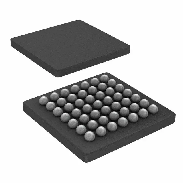
2112 logic elements in a 3.11×3.19 mm WLCSP
The LCMXO2-2000ZE-1UWG49ITR1K is a Lattice MachXO2 FPGA packing 2112 logic elements (264 LABs/CLBs) and 75 Kbit of embedded RAM into a 49-ball WLCSP measuring 3.11×3.19 mm — the smallest footprint in the MachXO2 family for this density tier. With 40 user I/O, this part is sized for glue-logic consolidation, bus bridging, or control-plane sequencing in space-constrained designs where a larger BGA or QFP would not fit the board outline.
Industrial temperature range and package integration
The 49-WLCSP (wafer-level chip-scale package) eliminates the mold compound and substrate — the die backside is the package top. The 3.11×3.19 mm body with 0.4 mm typical ball pitch demands a controlled impedance PCB with microvia fan-out under the balls; the land pattern matches the supplier device package drawing exactly.
Because this is a chip-scale package, the date-code and top-mark laser etch are the primary authentication points. The marking font, position, and ink-jet dot matrix pattern should match the Lattice wafer fab's standard for the reported week — any deviation flags potential re-mark or counterfeit material. Sourced per RFQ through independent distribution with full lot traceability.