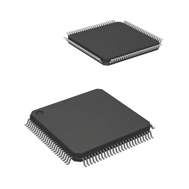
Lattice Semiconductor Corporation LCMXO2-1200HC-5TG100I — FPGA / CPLD & Programmable Logic
Technical Documents PDF / CAD
RoHS Compliant · Lead-Free EIA-481 Standard
Lattice Semiconductor Corporation / FPGA / CPLD & Programmable Logic

LCMXO2-1200HC-5TG100I Lattice MachXO2 FPGA, 1280 LUTs

MPN LCMXO2-1200HC-5TG100I
Active Spot Stock · 24-48h Dispatch 100% Original Sealed

Lattice Semiconductor MachXO2 FPGA, LCMXO2-1200HC-5TG100I, 1280 logic cells, 79 I/O, 64 Kbit RAM, 100-TQFP, -40 to 100°C, Tray.

In Stock: 680 pcs
MOQ: 1 pcs
Logistics: DHL / FedEx DAP (Global Express · 3-7d) Russia & CIS DDP (Door-to-Door Cleared)
Dispatch: Shenzhen / HK
Unit Price (USD)
$14.50 / pc
Direct Purchase Ready
Volume Pricing Breaks Confirmed upon quotation
1+ pcs
$14.50
10+ pcs
$13.05
30+ pcs
$11.89
100+ pcs
$10.73
500+ pcs
$10.01
Working on a production BOM or have a target unit price? Submit Target Price
Buy Now

$14.50 / ea

680 in stock — maximum per order · 3–4 days lead time

$13.05 / ea from 10 pcs

Upload Full BOM List
[SPEC] Essential Parameters Snapshot Full Specifications (10)
Package / Case 100-LQFP
Supply Voltage 2.375V ~ 3.465V

Full Technical Specifications

10 Parameters
LCMXO2-1200HC-5TG100I specifications
Parameter / AttributeSpecification / Value
SeriesMachXO2
MountingSurface Mount
Supply voltage2.375V ~ 3.465V
Operating temperature-40°C ~ 100°C (TJ)
PackageTray
Number of i (O)79
Case100-LQFP
Total RAM bits65536
Number of LABs (CLBs)160
Number of logic elements (Cells)1280
Series Sibling Variants

Lattice Semiconductor Corporation MachXO2 Series Models

Sibling variants, package options, and speed/density grades in this Lattice Semiconductor Corporation semiconductor series. Active Shenzhen warehouse allocation and rapid 24-48h dispatch.

Technical Details & Description

1280 logic cells, 79 I/O — density and interface width

The LCMXO2-1200HC-5TG100I packs 1280 logic cells (LUTs) in a 100-TQFP package, giving you 79 user I/O pins to connect to sensors, displays, or a host processor. That cell count lands it in the lower-mid density tier of the MachXO2 family — enough for glue logic, state machines, or a small MCU bus bridge without blowing the BOM on a larger FPGA. On-chip RAM totals 64 Kbit (65536 bits), enough for a small FIFO, coefficient lookup table, or boot-time scratchpad. The 160 logic blocks (LABs/CLBs) give the routing fabric room to pack the design without congestion.

Industrial temp and wide supply — fits harsh and mixed-voltage boards

The 100-TQFP (14x14 mm) package is a standard fine-pitch QFP with 0.5 mm lead pitch. It routes out on a 2-layer board for most designs, though a 4-layer stack-up helps with the core and I/O supply decoupling. The exposed pad on the bottom is not present — thermal management relies on airflow and the board copper.

Active lifecycle and compliance — no end-of-life risk for new designs

The base product number LCMXO2-1200 covers the whole die; the suffix -5TG100I denotes the speed grade (5 = standard), package (TG100 = 100-TQFP), and temperature range (I = industrial). The -4 and -6 speed grades share the same footprint and pinout, so a board spun for this part can accept a faster or slower sibling without a layout change.

Frequently asked questions

Will LCMXO2-1200HC-5TG100I drop into a board designed for LCMXO2-1200HC-4TG100I without rewiring?

Yes — the -4TG100I and -5TG100I share the same die, package (100-TQFP), pinout, and I/O count (79). The only difference is the speed grade: the -5 is the standard-speed bin, while the -4 is one notch slower. A board laid out for the -4 accepts the -5 without any PCB change.

What compliance documentation does Lattice provide for this part?

The LCMXO2-1200HC-5TG100I is ROHS3 Compliant (EU 2015/863). Lattice publishes a full material declaration and conflict-minerals report for the MachXO2 series. No UL or IEC certification is listed in the standard product specs.

LCMXO2-1200HC-5TG100I
Verified Allocation
Quote