Logic capacity and I/O budget for the 484-FBGA
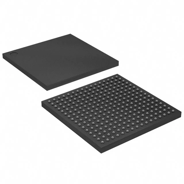
The EP4CE40F23C8L: The 39600 LE count positions it as a mid-density device in the Cyclone IV family, suitable for logic-intensive glue logic, motor-control interfaces, or sensor-fusion pipelines where a soft-core processor and peripheral bus fit within the available fabric. The 328 I/O are distributed across the 484-ball array on a 1.0 mm pitch. Routing all 328 signals out of the 23×23 mm package demands at least a six-layer PCB with buried vias for the inner rows; a four-layer board typically breaks out only the outer two ball rings, limiting usable I/O to about 180–200 pins.
On-chip memory and core supply
The 1161216 RAM bits are organized as M9K blocks — each block is 9 Kbit true dual-port. For a 32-bit wide FIFO at 100 MHz, the available blocks provide roughly 36 K words of buffer depth before you need external SRAM. The core voltage range of 0.97 V to 1.03 V is a narrow window: a 1.0 V rail with ±3% regulation keeps the core within spec, but a standard 1.0 V ±5% supply risks the low end at 0.95 V. For a fan-cooled enclosure with ambient below 50°C and typical logic utilization under 70%, the junction stays well within this band. If the board sits in a sealed box above 60°C ambient, a heatsink or forced air is required to keep the die below the 85°C ceiling.
Production status and supply posture
No stock-holding claim is made; the part is procured per RFQ.