Logic density and I/O bank planning
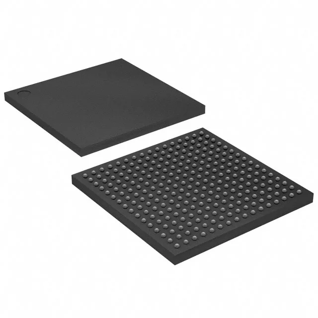
The EP4CE10F17I8L: 179 user I/O in a 256-FBGA (17x17) package means the I/O-to-package ratio is high: roughly 70% of the balls are signal pins, leaving the rest for supply and ground. That many I/O on a 17 mm body demands careful decoupling placement under the BGA — the four centre rows are power/ground, and the outer two rings carry the I/O banks. Each I/O bank runs on its own VCCIO rail (1.2 V to 3.3 V), so the same device can interface a 1.8 V DDR memory on one bank and 3.3 V peripherals on another without external level shifters — but the bank assignment must match the PCB layout before the route starts.
Industrial temperature grade and core voltage tolerance
The 100°C TJ ceiling means the device can run in an unventilated enclosure near a 70°C ambient if the thermal resistance of the 256-FBGA package is managed with forced air or a heat spreader. Core supply is 0.97 V to 1.03 V — a tight 60 mV window. A 1.0 V switching regulator with ±3% set-point accuracy stays inside this band, but a 1.2 V rail with a linear regulator drops too much headroom. The low core voltage keeps dynamic power down: at 100 MHz the core draws roughly 1.5 mW per LE, so the 10k-LE device runs under 200 mW typical.
On-chip memory and block RAM distribution
423936 bits of total RAM — that is 414 Kbit, organised as M9K memory blocks (9 Kbit each). Forty-six blocks are available, each configurable as single-port, simple dual-port, or true dual-port RAM, ROM, or FIFO. A 32-deep, 18-bit-wide FIFO uses one block; a 512x8 buffer uses two. The total is enough for a small packet buffer or coefficient table but not for a full frame store.