Logic density and I/O count for the BOM line
The 10M02SCE144A7G is an Intel MAX® 10 FPGA with 2000 logic elements arranged across 125 LABs/CLBs, giving it the gate count to handle glue logic, sensor fusion, or a small state machine without an external CPLD. 101 user I/O pins break out from the 144-LQFP Exposed Pad package — enough for a 16-bit data bus, address lines, and a handful of control signals, with margin for a parallel LCD or external SRAM interface.
Package and thermal path
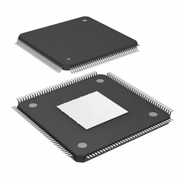
144-LQFP Exposed Pad, also designated 144-EQFP (20x20 mm). The 0.50 mm pitch on the LQFP demands a 4-layer board for reliable fan-out of the inner rows; a 2-layer board will struggle to route all 101 I/O without via-in-pad or blind vias.
On-chip memory and block RAM budget
110592 total RAM bits — roughly 13.5 KB — serve as block RAM for FIFOs, line buffers, or small look-up tables. Enough for a 128x64 pixel frame buffer at 1 bpp, or a 256-entry coefficient table for a digital filter.