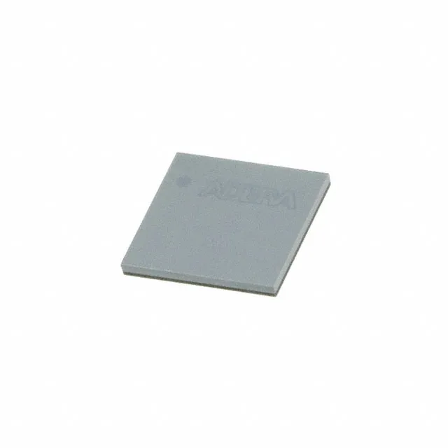
Intel 10M02DCV36C7G — FPGA / CPLD & Programmable Logic

Intel 10M02DCV36C7G MAX 10 FPGA, 2000 LE, 27 I/O, WLCSP

MPN10M02DCV36C7G
Active

Intel MAX® 10 FPGA, 10M02DCV36C7G, 2000 logic elements, 27 I/O, 110592 total RAM bits, 1.15V–1.25V core supply, 0°C to 85°C operating temperature, 36-UFBGA WLCSP package.

$4.1500Ref. price · indicative, final on quote
Packaging36-UFBGA, WLCSP
RoHSRoHS Compliant
SeriesMAX® 10
Independent supplier — new & surplus stockAuthenticity-screened · ESD-safe packingListing updated Aug 2026

Specifications

10M02DCV36C7G specifications
ParameterValue
SeriesMAX® 10
MountingSurface Mount
Voltage1.15V ~ 1.25V
Operating temperature0°C ~ 85°C (TJ)
PackageTape & Reel (TR)
Number of i (O)27
Case36-UFBGA, WLCSP
Total RAM bits110592
Number of LABs (CLBs)125
Number of logic elements (Cells)2000

Product details

2000 logic elements — capacity ceiling for your gate count

2000 logic elements and 125 LABs/CLBs handle small state machines, address decoding, or counter/timer blocks. It will not fit a soft-core CPU or video scaler.

RoHS compliant.

Temperature grade — indoor use only

Rated 0°C to 85°C (TJ). This is the commercial grade. The part will not operate below freezing or in an enclosure that sees direct sun or engine-bay heat. For extended-temperature designs, the MAX 10 family offers -40°C to 125°C variants (e.g., 10M02SCE144A7G) in larger packages. If your BOM requires industrial or automotive temperature, this is not the correct order code.

Frequently asked questions

What is the operating temperature of 10M02DCV36C7G?

The operating temperature range is 0°C to 85°C (TJ), commercial grade.

What is the equivalent of 10M02DCV36C7G?

The 10M02SCE144C8G is a functional equivalent with the same 2000 logic elements and 110592 RAM bits, but in a 144-ball EQFP package with 101 I/O — it is not pin-compatible.

Is 10M02DCV36C7G compatible with 1.8V I/O?

The I/O banks can be configured for 1.8V, 2.5V, or 3.3V operation depending on the VCCIO supply assignment, but per-bank voltage details require the pinout diagram to confirm.