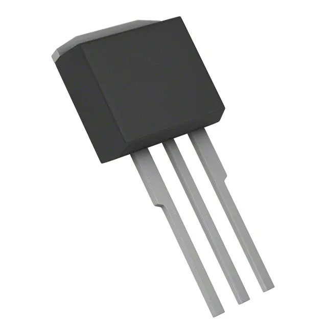
HEXFET N-channel, 100 V, 36 A — TO-262 through-hole
It is offered in a TO-262 (I²Pak) through-hole package with long leads, suited for board-level power switching where a robust, solderable through-hole mount is preferred over surface-mount for thermal or mechanical reasons.
Rated for harsh environments
This makes it a candidate for applications that see extreme thermal cycling — engine bay electronics, industrial motor drives, downhole instrumentation, or avionics power stages where the ambient may exceed 125°C. The 175°C maximum junction allows derating headroom for high-current, high-ambient designs.
Switching and drive characteristics
Gate charge (Qg) is 74 nC at 5 V, and input capacitance (Ciss) is 1800 pF at 25 V drain-source. These numbers are moderate for a 100 V / 36 A device — the gate driver sees a manageable capacitive load, and switching losses at moderate frequencies (tens of kHz) are reasonable. The drive voltage range (4 V to 10 V for achieving rated Rds(on)) means a 5 V logic output can turn the device on, but the 10 V rating for minimum Rds(on) is typical for logic-level FETs; a 10 V gate supply will give the lowest conduction loss. Maximum gate-source voltage is ±16 V, so standard 12 V gate drive rails are safe.
Obsolete — sourcing strategy
New designs should not specify this part; for existing BOM lines, procurement must rely on the independent and surplus distribution channel. No official replacement part number is listed in the manufacturer's lifecycle record for this specific variant, so any substitution requires a full parametric and footprint review.
Power dissipation and thermal design
Maximum power dissipation is 3.8 W at ambient (Ta) and 140 W at case (Tc). In practice, the TO-262 package's tab is the primary heat path; a properly soldered through-hole joint to a copper plane or an external heatsink is essential for continuous operation above a few amps. The 36 A continuous drain current rating is also at Tc = 25°C; derate for real-world case temperatures.