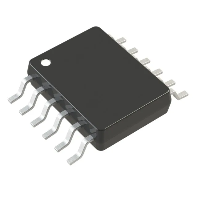
Analog Devices LTC2644HMS-L12#PBF — Logic ICs
Technical Documents PDF / CAD
RoHS Compliant · Lead-Free EIA-481 Standard
Analog Devices / Logic ICs

LTC2644HMS-L12#PBF Dual 12-Bit PWM DAC, 7.8µs

MPN LTC2644HMS-L12#PBF
End of Life Spot Stock · 24-48h Dispatch 100% Original Sealed

Analog Devices LTC2644HMS-L12#PBF, dual 12-bit voltage-output DAC, PWM data interface, 7.8µs typ settling, ±1 LSB INL/DNL, 2.7V to 5.5V supply, -40°C to 125°C, 12-MSOP package, Tube.

In Stock: 16 pcs
MOQ: 1 pcs
Logistics: DHL / FedEx DAP (Global Express · 3-7d) Russia & CIS DDP (Door-to-Door Cleared)
Dispatch: Shenzhen / HK
Unit Price (USD)
$16.30 / pc
Direct Purchase Ready
Volume Pricing Breaks Confirmed upon quotation
1+ pcs
$16.30
10+ pcs
$15.57
Working on a production BOM or have a target unit price? Submit Target Price
Buy Now

$16.30 / ea

16 in stock — maximum per order · 3–4 days lead time

$15.57 / ea from 10 pcs

Upload Full BOM List
[SPEC] Essential Parameters Snapshot Full Specifications (14)
Package / Case 12-TSSOP (0.118", 3.00mm Width)
Supply Voltage 2.7V ~ 5.5V

Full Technical Specifications

14 Parameters
LTC2644HMS-L12#PBF specifications
Parameter / AttributeSpecification / Value
Output typeVoltage - Buffered
MountingSurface Mount
Reference typeExternal, Internal
Voltage - supply, analog2.7V ~ 5.5V
Voltage - supply, digital2.7V ~ 5.5V
Data interfacePWM
Operating temperature-40°C ~ 125°C
PackageTube
INL (DNL)±1, ±1 (Max)
Settling time7.8µs (Typ)
Number of bits12
Case12-TSSOP (0.118\", 3.00mm Width)
Differential outputNo
Number of d (A converters)2
[DESK] Shenzhen Spot Allocation · 2h Response

Need Immediate Spot Stock or Shortage Allocation for LTC2644HMS-L12#PBF?

Factory lead times blocking production? We lock verified brand-new original stock in Shenzhen within 2 hours.

Quote SLA 2 Hours
[01] Emergency Shortage 24-48h Shenzhen Dispatch

Direct access to Shenzhen floor inventory, franchised allocation buffers, and factory bonded stock to resolve line-down shutdowns.

[02] Industrial Packaging Tape & Reel / Tray / Tube

Standard factory-sealed packaging compliant with EIA-481 standards for automated high-speed SMT pick-and-place lines.

[03] WhatsApp QC Proof 45x Microscope QC Photos

High-resolution photos of original reel labels, 2D DataMatrix, and pin coplanarity sent via WhatsApp/Telegram before you release wire payment.

● USD Wire Transfer (SWIFT T/T) · DAP Express / DDP Delivery

Technical Details & Description

Dual 12-bit PWM DAC with extended temperature range

It integrates two DAC channels in a 12-MSOP package, each with its own PWM demodulator and output buffer, so a single PWM signal per channel generates a clean analog voltage without an external filter.

The data interface is PWM, not SPI or I2C. That is the defining difference versus most precision DACs: you feed a variable-duty-cycle digital signal on each channel's PWM input, and the internal demodulator converts it to a DC voltage. The settling time to 0.5 LSB is 7.8 µs typ, which sets the minimum PWM period you can use. If your PWM carrier runs at, say, 1 kHz (1 ms period), the DAC settles well within one cycle. At higher PWM frequencies — 100 kHz gives a 10 µs period — the 7.8 µs settling consumes most of the period, so the output may not fully settle before the next update. For closed-loop applications, budget the settling time against your PWM update rate.

Accuracy budget: ±1 LSB INL and DNL

Integral and differential nonlinearity are both specified at ±1 LSB maximum at 12 bits. That means every code is guaranteed monotonic, and the worst-case deviation from an ideal transfer function is one LSB — about 0.024% of full scale at 5 V reference. No calibration is needed for most 12-bit systems; if your error budget allocates ±0.1% for the DAC, this part fits without trimming. The reference can be external or internal, so you can match the full-scale range to the ADC reference or sensor output span.

Package and supply: 12-MSOP footprint, single-supply operation

Housed in a 12-MSOP (3.00 mm × 3.00 mm body, 0.65 mm pitch), this DAC fits on dense mixed-signal boards where every mm² counts. The output is rail-to-rail buffered, swinging from near ground to within a few millivolts of the positive rail. Surface-mount assembly is standard; no exposed pad to route.

For volume commitments or scheduled deliveries, a procurement inquiry will establish lead time and price breaks.

Frequently asked questions

Does LTC2644HMS-L12#PBF have a SPI or PWM interface?

The data interface is PWM, not SPI. Each of the two DAC channels accepts a separate PWM input, and the internal demodulator converts the duty cycle to a buffered analog voltage.

What is the output type of the LTC2644?

The output is Voltage - Buffered, meaning each DAC channel has an internal rail-to-rail output buffer that can drive loads directly without an external op-amp.

What are the equivalent replacement parts for LTC2644HMS-L12#PBF?

The AD5689RBRUZ and AD5689RARUZ are 16-bit dual DACs from the same nanoDAC+ family with SPI interface, but they are not pin-compatible (different package and interface). The AD7249ARZ is a 12-bit dual DAC with SPI interface in a wider SOIC package. None of these are drop-in replacements — the LTC2644's PWM input is unique. For a functional equivalent with the same PWM interface, stay within the LTC2644 family.

LTC2644HMS-L12#PBF
Verified Allocation
Quote