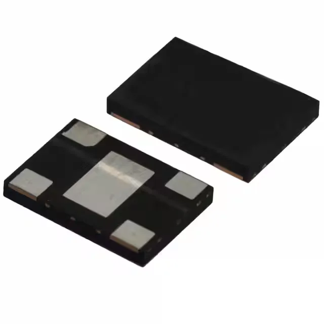
133.333 MHz LVCMOS clock from a Pure Silicon MEMS resonator
The ASVMB-133.333MHZ-XY-T is a standard XO from Abracon's Pure Silicon series — it uses a MEMS resonator rather than a traditional quartz crystal, which eliminates the mechanical fragility of crystal blanks and gives tighter initial tolerance over temperature. The output is LVCMOS, the default logic standard for most MCUs, SoCs, and FPGAs — the 133.333 MHz frequency is a common reference clock for Ethernet PHY, USB-PHY, and PCIe-adjacent SerDes stages, so this part sits behind a lot of connectivity silicon without needing a level translator. Frequency stability of ±10ppm keeps accumulated clock error below the typical USB 500 ppm budget for a full day of operation, and well within the ±50 ppm window that most telecom PHY clocks require as a system-level allocation.
Voltage flexibility and power budget for battery and wired designs
A single LDO that already supplies the digital core can feed this oscillator directly. Active supply current peaks at 16 mA; in standby (power-down mode) it drops to 15 µA. The 1,000× ratio means a battery-powered design can park the clock in standby between transmission bursts and recover timing within the MEMS startup spec without draining the rail continuously.
Package and thermal profile for board-level layout
The exposed paddle under the device is the primary thermal and ground reference path — it should be soldered to the PCB land, not left floating, to achieve the datasheet frequency stability specification. A junction temperature analysis is still required if the device is located near a hot regulator or processor.