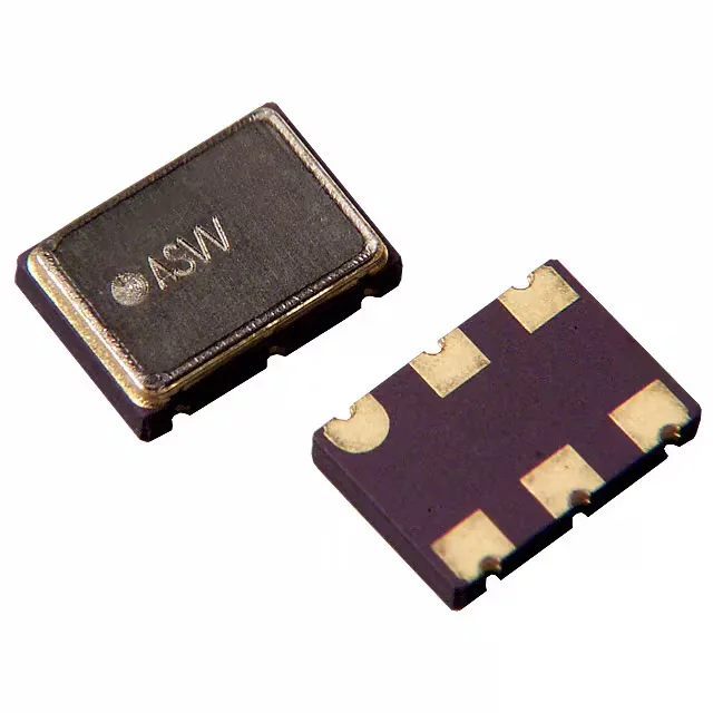
What the ASVV series delivers at 61.44 MHz
The ASVV-61.440MHZ-C25-N102-T: That dual-output flexibility means the same device clocks a 3.3 V TTL CPLD or FPGA input on one side and a CMOS-compatible PHY or SerDes reference on the other, without changing the component on the BOM line. For a 61.44 MHz clock, that translates to a worst-case deviation of about ±1.54 kHz, which sits comfortably within the timing margin of most UART, SPI, and lower-speed SERDES interfaces. If your link budget is tighter than that, you would reach for a TCXO or OCXO instead; the VCXO form factor is sized for boards where moderate stability at lower cost is the design goal. The standby (power-down) function lets the oscillator's internal output stage go high-impedance on a control pin, effectively disconnecting the clock from downstream logic without removing the supply voltage. A system that gates clocks to reduce power during a low-power mode uses this pin rather than switching the supply rail — the VCXO remains biased and can re-lock faster than a cold-start oscillator.
Package and PCB integration
The no-lead footprint lands on a standard 0.5 mm pitch grid — route out from the four sides and tie the GND pad beneath the body to the ground plane through thermal vias. The exposed pad is the ground reference for the oscillator's internal circuitry; it is not a thermal relief path but a DC reference, so do not float it. Supply current peaks at 35 mA — not a large number, but the VCXO's internal PLL draws a burst of current on each output edge. Decouple the 3.3 V rail with a 100 nF ceramic close to the package pins and a second 1 µF bulk cap within 5 mm; this keeps the supply noise below the PLL's rejection floor and prevents frequency modulation of the output from rail sag. Supplied on Tape & Reel, the device is compatible with standard SMT pick-and-place. No dry-pack or MSL rating is stated in the listing — confirm with the supplier whether the reel as received is desiccant-sealed if your board assembly line applies pre-bake moisture thresholds.
The ASVV family is an established commercial timing line; sourcing runs through authorized distribution and independent channels as quantities allow. No official second-source or pin-compatible successor is cited in the listing. The 61.44 MHz frequency and the specific ±25 ppm stability grade narrow the field — if you are writing a second-source clause into the BOM, confirm the load capacitance and control voltage range of any alternative VCXO match before listing it as equivalent. A different manufacturer may specify the same nominal frequency but require a different VCOTUNE voltage range to achieve the same pull range.