SI2387DS-T1-GE3

Vishay · TrenchFET® Gen IV Series

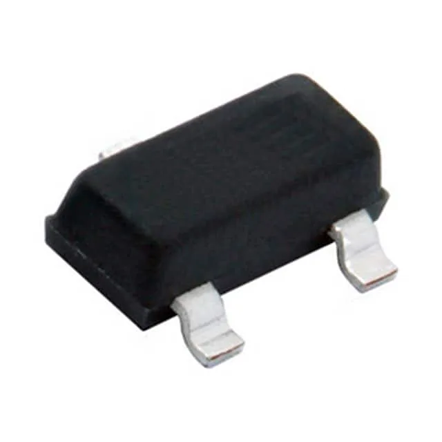
Vishay TrenchFET® Gen IV P-Channel MOSFET, SI2387DS-T1-GE3, 80 Vdss, 2.1 A continuous drain, 164 mOhm Rds(on) at 10 V, SOT-23-3 surface mount, Tape & Reel.

Vishay SI2387DS-T1-GE3
Download datasheet (PDF)
[IN STOCK] In Stock: 228 pcs
$12.60/ pc

Volume pricing

Buy Now

MOQ 1 · Tape & Reel (TR); Cut Tape (CT) · RoHS · EIA-481 · DAP/DDP · T/T

Technical specifications

SI2387DS-T1-GE3 specifications
Parameter / AttributeSpecification / Value
SeriesTrenchFET® Gen IV
FET typeP-Channel
MountingSurface Mount
Drain to source voltage80 V
Drive voltage (Max rds on, min rds on)4.5V, 10V
Current - continuous drain (Id) @ 25°C2.1A (Ta), 3A (Tc)
Power dissipation1.3W (Ta), 2.5W (Tc)
Operating temperature-55°C ~ 150°C (TJ)
PackageTape & Reel (TR); Cut Tape (CT)
Vgs±20V
TechnologyMOSFET (Metal Oxide)
CaseTO-236-3, SC-59, SOT-23-3
Vgs(th) (Max) @ id2.5V @ 250µA
Rds on (Max) @ id, vgs164mOhm @ 2.1A, 10V
Gate charge (Qg) (Max) @ vgs10.2 nC @ 10 V
Input capacitance (Ciss) (Max) @ vds395 pF @ 40 V

Technical details

The SI2387DS-T1-GE3: Gate charge is 10.2 nC at 10 V, and input capacitance is 395 pF at 40 V Vds — these numbers tell you the switching speed is limited more by the gate-drive source resistance than by the FET itself; a 10-ohm driver delivers sub-100 ns rise times.

SOT-23-3 footprint and board integration

The SOT-23-3 (TO-236) package occupies a 2.9 mm × 1.3 mm footprint — the drain is the centre pin, source and gate on the outer pins. The exposed die attach pad is the drain terminal; the PCB copper area under the pad sets the thermal resistance to ambient. Drive voltage range is 4.5 V minimum for the rated on-resistance, though the 10 V figure gives the lowest Rds(on); at 4.5 V the on-resistance will be higher than the 164 mOhm spec — check the typical curve if driving from a 3.3 V logic rail.

SI2387DS-T1-GE3
[ALLOC] verified
Quote