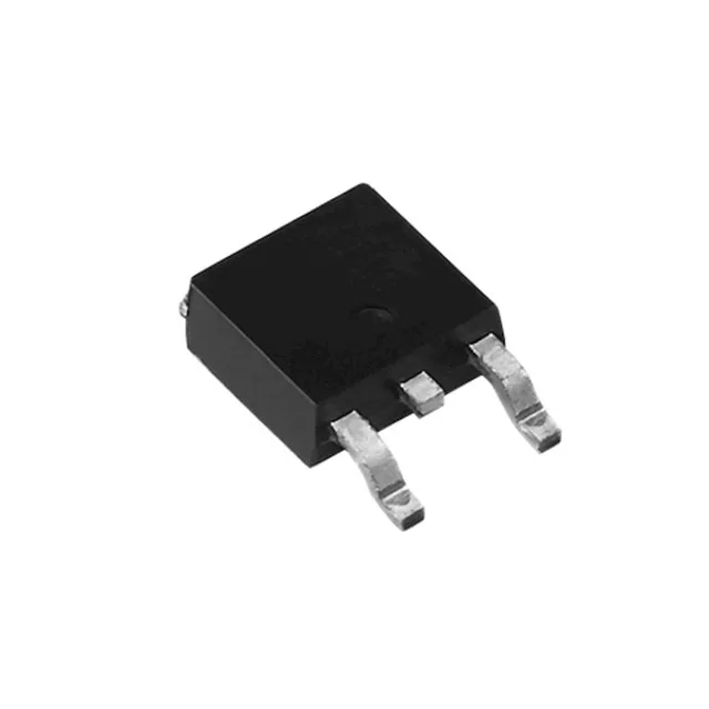
It comes in a surface-mount DPAK (TO-252-3) package, making it suitable for high-voltage switching applications such as AC-DC converters, power factor correction stages, and motor drives where board space is constrained. The device supports a gate drive voltage of 10 V for minimum on-resistance, with a maximum Rds(on) of 309 mOhm at 7 A and 10 V.
Ratings that drive the design — Rds(on), gate charge, and thermal margin
The 309 mOhm Rds(on) at 7 A and 10 V is the figure to use for conduction-loss calculations at operating temperature — the 25 °C value in the datasheet will roughly double at 125 °C junction, so budget accordingly. Input capacitance is 1205 pF at 100 V Vds, a moderate value that doesn't demand an aggressive gate-drive stage but still benefits from a low-impedance path to avoid ringing. Maximum power dissipation is 147 W at case temperature, though real-world dissipation will be limited by the PCB's ability to sink heat through the DPAK's exposed pad. The maximum gate-source voltage is ±30 V, which is generous for a 600 V part and reduces the risk of oxide breakdown during transients.
Lifecycle and compliance — active status with no LTB risk
The part is RoHS compliant, as indicated by the GE3 suffix.