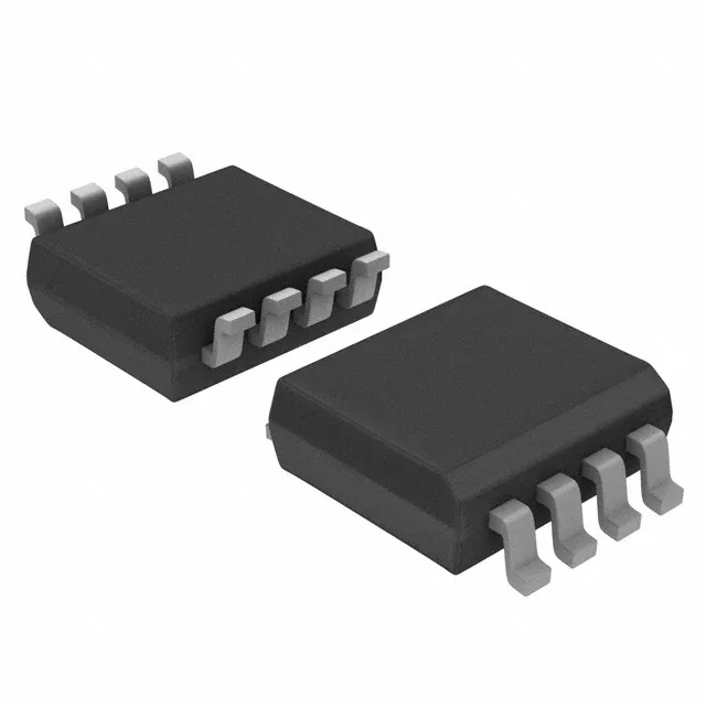
Toshiba Semiconductor TC7W00FK,LF — Discrete Semiconductors
Technical Documents PDF / CAD
RoHS Compliant · Lead-Free EIA-481 Standard
Toshiba Semiconductor / Discrete Semiconductors

Toshiba TC7W00FK,LF NAND Gate IC, 2V-6V, 8-SSOP

MPN TC7W00FK,LF
End of Life Spot Stock · 24-48h Dispatch 100% Original Sealed

Toshiba TC7W series dual 2-input NAND gate, 8-VFSOP (2.30mm width) surface-mount package, 2V to 6V supply, 1 µA quiescent current, 13ns propagation delay at 6V, 50pF.

In Stock: 2,835 pcs
MOQ: 1 pcs
Logistics: DHL / FedEx DAP (Global Express · 3-7d) Russia & CIS DDP (Door-to-Door Cleared)
Dispatch: Shenzhen / HK
Unit Price (USD)
$0.40 / pc
Direct Purchase Ready
Volume Pricing Breaks Confirmed upon quotation
1+ pcs
$0.40
10+ pcs
$0.36
30+ pcs
$0.33
100+ pcs
$0.30
500+ pcs
$0.28
1,000+ pcs
$0.26
Working on a production BOM or have a target unit price? Submit Target Price
Buy Now

$0.40 / ea

2,835 in stock — maximum per order · 3–4 days lead time

$0.36 / ea from 10 pcs

Upload Full BOM List
[SPEC] Essential Parameters Snapshot Full Specifications (14)
Package / Case 8-VFSOP (0.091", 2.30mm Width)
Supply Voltage 2V ~ 6V
Output / Current 5.2mA, 5.2mA

Full Technical Specifications

14 Parameters
TC7W00FK,LF specifications
Parameter / AttributeSpecification / Value
SeriesTC7W
Logic typeNAND Gate
MountingSurface Mount
Supply voltage2V ~ 6V
Current - quiescent1 µA
Current - output high, low5.2mA, 5.2mA
I/O channels2
Operating temperature-40°C ~ 85°C
PackageTape & Reel (TR); Cut Tape (CT)
Case8-VFSOP (0.091\", 2.30mm Width)
Number of circuits2
Input logic level - low0.5V ~ 1.8V
Input logic level - high1.5V ~ 4.2V
Max propagation delay @ v, max CL13ns @ 6V, 50pF
Series Sibling Variants

Toshiba Semiconductor TC7W Series Models

Sibling variants, package options, and speed/density grades in this Toshiba Semiconductor semiconductor series. Active Shenzhen warehouse allocation and rapid 24-48h dispatch.

Technical Details & Description

Dual NAND gate in a tight 8-pin SSOP

The TC7W00FK,LF is a dual 2-input NAND gate from Toshiba's TC7W series, packing two independent gates into an 8-VFSOP package that measures 2.30 mm wide — the 8-SSOP footprint fits into dense mixed-signal boards where board real estate is the bottleneck. Quiescent current maxes out at 1 µA — negligible in battery-powered logic where every microamp counts.

Propagation delay and drive capability

Max propagation delay is 13 ns at 6V with a 50 pF load — that's the worst-case figure across temperature and voltage. At 5V the delay tightens; for timing-sensitive paths, budget the 13 ns ceiling and check the actual load capacitance on the trace. Output drive is symmetric at 5.2 mA source and sink — enough to switch a downstream CMOS gate input or a low-power LED indicator, but not enough to drive a relay coil or a long bus without a buffer. Logic thresholds are specified as input-low at 0.5V to 1.8V and input-high at 1.5V to 4.2V across the 2V-6V supply range — the overlap region (1.5V to 1.8V) is the undefined zone; keep input rise/fall times fast enough to avoid oscillation there.

Package, temperature grade, and compliance

Housed in an 8-VFSOP (0.091" body width, 2.30 mm) with supplier device package designation 8-SSOP. Surface-mount only — the fine-pitch leads need a hot-air rework station with a fine nozzle; a standard soldering iron tip is too wide for the pad spacing.

Frequently asked questions

What is the closest functional alternative to the TC7W00FK,LF?

The TC7W08FKTE85LF is the AND-gate sibling in the same TC7W series — same package, same supply range, same pinout. The logic function differs (AND vs NAND), so the board-level swap requires checking the downstream logic. The TC7W04FK,LF is a triple inverter in the same family and package but with three circuits instead of two.

What compliance documentation does Toshiba provide for the TC7W00FK,LF?

The part is ROHS3 compliant per the lifecycle record.

TC7W00FK,LF
Verified Allocation
Quote