Fixed 4.3V rail — the niche that defines the fit
The TLV70243DSET is a fixed 4.3 V output LDO from TI's TLV702 family, rated for 300 mA continuous. That output voltage sits between the common 3.3 V and 5.0 V rails — it is not a general-purpose regulator; it is specced into a design that needs exactly 4.3 V, likely to bias an analog front-end or a specific sensor bridge where the 1.2 V headroom above 3.3 V matters for PSRR margin. With a 5.0 V input bus, that is 325 mV of headroom — comfortable for a clean rail, tight if the 5 V bus itself sags under transient load.
PSRR and quiescent — the analog-rail trade-off
PSRR is 68 dB at 1 kHz — this attenuates switching-regulator ripple at the typical 1 MHz fundamental by roughly 30-40 dB (the roll-off is about 20 dB/decade past the unity-gain crossover). For a 10 mVpp ripple on the input, the output sees roughly 3 µVpp at 1 kHz, clean enough for a 12-bit ADC reference or a sensitive analog supply. Below 100 Hz the PSRR is higher, but the real noise threat is the switching frequency band. Quiescent current is 55 µA typical, with a max supply current of 370 µA. For a battery-powered sensor node that spends most of its time in sleep, the 55 µA Iq is the dominant drain — it sets the floor for standby battery life. An always-on 4.3 V rail drawing 55 µA from a 200 mAh coin cell gives about 150 days of standby before the regulator's own consumption drains the cell.
Protection set and temperature grade
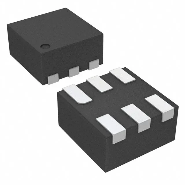
The TLV70243DSET integrates over-current, over-temperature, reverse polarity, and under-voltage lockout (UVLO) protection. The UVLO threshold is typically around 1.6 V rising — below that the output is held off, preventing the pass FET from operating in the linear region during a brownout. Reverse polarity protection means a reversed input rail does not damage the regulator (the body diode of the pass FET blocks the reverse current). The 6-WSON package (1.5x1.5 mm) has a thermal pad on the bottom — the datasheet layout recommendation is a 2x2 via array under the pad to the ground plane. Without that thermal via pattern, the effective RθJA rises by roughly 30%, and at 125°C ambient the 300 mA load pushes the junction close to the 150°C abs-max limit.