The TLV70028DSER delivers 68 dB of power-supply rejection at 1 kHz, which means it attenuates switching ripple from a typical buck converter by a factor of roughly 2500. If the upstream rail carries 10 mVpp of 1 MHz ripple, the output sees under 4 µVpp — clean enough for an analog front-end or a precision reference supply. PSRR rolls off above the crossover frequency set by the error amplifier bandwidth; at 100 kHz the rejection is lower, so the input filter ahead of the LDO still matters if the switcher runs above 500 kHz.
200 mA output, 250 mV dropout — the headroom rule
Rated for 200 mA continuous output with a maximum dropout voltage of 0.25 V at full load. The input rail must stay at least 250 mV above 2.8 V across the full load and temperature range — below that the pass transistor saturates and the output falls out of regulation. A 3.3 V rail gives 300 mV of headroom at room temperature, but at 125 °C the dropout voltage rises, so 3.0 V minimum input is the practical floor. The 55 µA quiescent current (270 µA max supply) keeps the regulator's own draw low enough for always-on rails in battery-powered equipment — a sensor node pulling 50 µA in sleep mode still sees the LDO's Iq as the dominant load.
6-WSON package — thermal and layout considerations
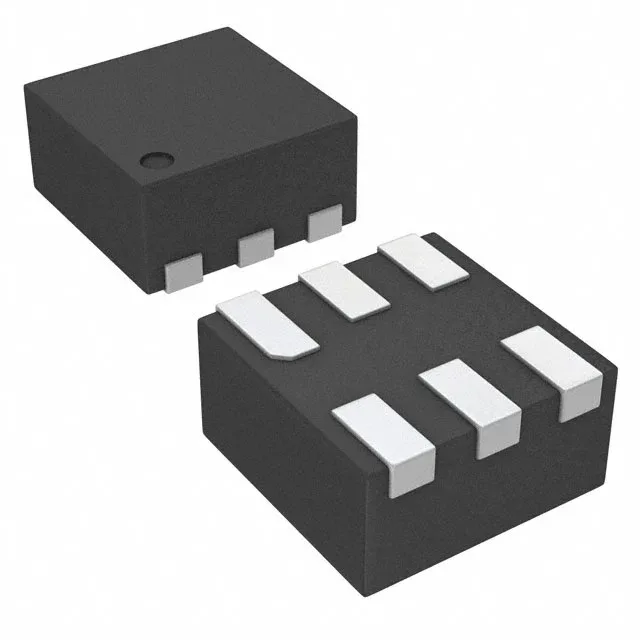
The 6-WFDFN package (6-WSON, 1.5x1.5 mm) has an exposed thermal pad on the bottom. The datasheet's RthJA figure assumes a copper land and thermal vias under the pad — without them the junction temperature rises faster than the 125 °C rating allows at full load in a 85 °C ambient. A 2x2 array of 0.3 mm vias under the pad is the standard layout practice. Surface-mount only — no through-hole variant. The small footprint means the board house must handle 0.5 mm pitch pads; a solder stencil with 0.125 mm aperture is typical for the exposed pad.
Protection suite — reverse polarity and UVLO
The TLV70028DSER integrates over-current, over-temperature, reverse polarity, and under-voltage lockout (UVLO) protection. The reverse polarity protection is notable — it blocks negative input voltages without an external Schottky diode, saving board space and BOM cost on the input rail. UVLO holds the output off until the input rises above the internal threshold, preventing brownout operation. The enable pin (active high) lets a GPIO or supervisor IC gate the output. When pulled low, the regulator enters shutdown and the output goes high-impedance — the load is not back-driven through the pass FET.