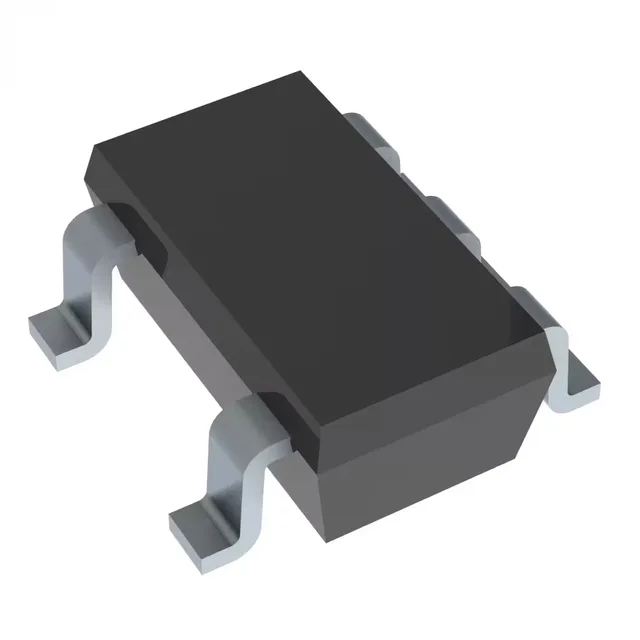
Open-drain inverter for level translation and wired-OR buses
The SN74AUP1G06DBVR is a single inverter from TI's 74AUP logic family, but the open-drain output sets it apart from a standard push-pull inverter — the output FET pulls low actively but floats high, relying on an external pull-up resistor to define the high-level voltage. The propagation delay is 10.5 ns at 3.3 V into 30 pF — fast enough for I²C clock stretching or general-purpose logic gating below 50 MHz.
Supply voltage and output drive — what the ratings mean for the BOM
Because the output is open-drain, the high-level voltage is set by the pull-up resistor's supply — this can be a different rail than VCC, enabling bidirectional level shifting without an external translator. Output low current is rated 4 mA, which is typical for the 74AUP family. The pull-up resistor value must be chosen so the output low voltage stays within the downstream logic's VIL threshold at that sink current. There is no output high current spec — the open-drain FET only sinks. Input logic thresholds are specified: low at 0.1 V to 0.45 V and high at 3.6 V. The wide low threshold range means the gate reliably interprets sub-0.45 V signals as low across the full supply range, which helps in noisy or slow-edge environments.
Package, footprint, and temperature grade
Housed in a SOT-23-5 (SC-74A) package, the SN74AUP1G06DBVR occupies minimal board area. The five-pin footprint — VCC, GND, input, output, and a no-connect — is standard for single-gate logic and routes easily on two-layer boards. This covers most indoor and outdoor equipment enclosures but not extended automotive under-hood environments. For a sensor node or IoT gateway that sees seasonal extremes, the 85°C ceiling is the limit to respect.