What AEC-Q100 Grade Means for Your BOM
The Texas Instruments BQ25171QWDRCRQ1 is an automotive-grade linear battery charger for single-cell to 6-cell Li-Ion or Li-Polymer packs. The 18V maximum supply gives enough headroom to ride through 12V load-dump transients without an external pre-regulator, which simplifies the power-stage BOM on an automotive ECU.
800 mA Linear Charge Current — Sizing the Thermal Budget
Maximum charge current is 800 mA, constant-current programmable via the ISET pin. In a linear topology, the pass element drops the difference between input and battery voltage. At 800 mA with a 12V input charging a 4-cell pack at 16.8V, the dissipation is roughly 4W — the 10-VSON with exposed pad needs a solid thermal via stitch to the ground plane to keep junction temperature below 125°C. For higher-current designs, this part is the low-cost linear option; a switching charger would be the next tier.
1 to 6 Cells — Application Fit
The charger handles 1 to 6 series cells with a maximum battery pack voltage of 10.5V. That covers 1S (4.2V) through 2S (8.4V) packs cleanly. For 3S and above the 10.5V ceiling is the limit — a 3S Li-Ion pack at 12.6V exceeds it, so this part is suited for up to 2S automotive auxiliary batteries, backup power for ADAS modules, or single-cell key-fob chargers. The programmable charge timer provides a safety timeout for fault conditions.
On-Die Fault Protections
Integrated fault protection covers over-current, over-temperature, over-voltage, and short-circuit conditions. Over-voltage protection is built in — no external clamping diode needed on the battery pin. Over-temperature shutdown protects the die during high-ambient or high-dissipation scenarios typical of under-hood placement. This protection set reduces the discrete component count around the charger IC.
Package and Mounting for Automotive Assembly
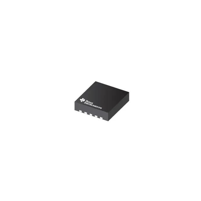
Supplied in Tape & Reel in a 10-VFDFN with wettable flank. The wettable flank enables automated optical inspection (AOI) of the solder joints — a requirement for many Tier-1 automotive lines. The 3x3 mm VSON footprint with an exposed pad requires a thermal-land pattern on the PCB; without it the 125°C junction limit will be reached at lower charge currents.