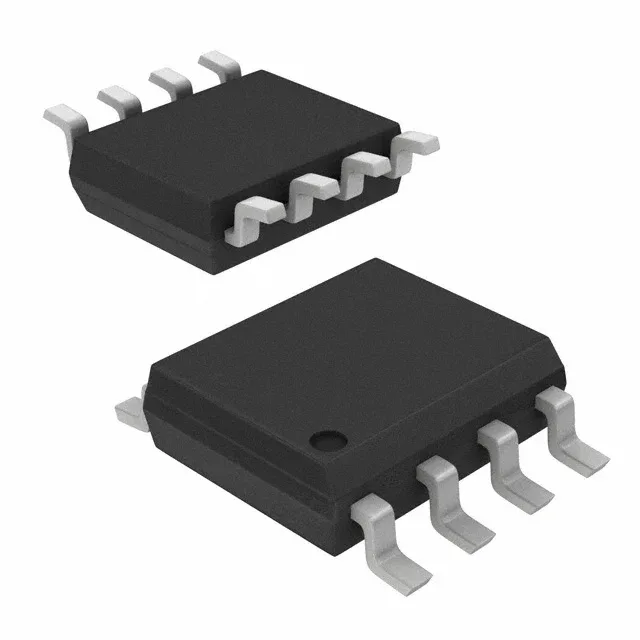
Package and board integration — 16-VQFN exposed pad
The RAA2261104GNP#HA0 comes in a 16-VQFN Exposed Pad package (4x4 mm, supplier device package 16-QFN). The exposed paddle on the bottom side is the primary thermal path — the PCB land pattern must include a thermal via array under the pad to pull heat into the inner copper planes. The 0.5 mm pitch on the perimeter lands requires a solder-mask-defined pad geometry; a 4-layer board with a solid ground plane under the driver is the typical starting point.
Driven configuration and output current — low-side GaN driver
This is a low-side driver with independent channels, designed to drive N-Channel MOSFET gates. The peak output current is 2 A source and 1.2 A sink — the asymmetry is intentional: the stronger pull-up charges the gate capacitance quickly for fast turn-on, while the weaker pull-down limits di/dt during turn-off to control ringing. The 30 ns rise and 31 ns fall times (typical) put the switching edge in the tens-of-nanoseconds range, which means the gate-loop inductance must stay under 10 nH to avoid voltage overshoot at the gate.
Supply range and temperature grade — 6.5 V to 18 V, -40 to 125 °C
The supply voltage range is 6.5 V to 18 V, covering the common bias rails for GaN gate drivers (typically 8 V to 12 V for enhancement-mode GaN FETs). The operating temperature range of -40 °C to 125 °C is the industrial-plus band — the part is rated for continuous operation at 125 °C ambient, so the junction temperature stays within the die rating even in a hot enclosure near the power stage. The logic input thresholds are 1.6 V (VIL) and 2.3 V (VIH), compatible with 3.3 V and 5 V logic families without a level shifter.
Active production and compliance
Renesas lists this part as Active with ROHS3 compliance. The part is available in Tape & Reel or Cut Tape options — the reel quantity is the standard 16-QFN carrier tape format. Quoted to order against the BOM; availability and current pricing confirmed at RFQ time.