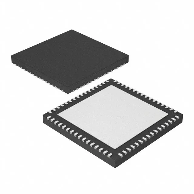
Renesas Electronics R7FA6T2AD3CNB#AA0 — Microcontrollers & Processors (MCU / MPU / DSP)

R7FA6T2AD3CNB#AA0 Renesas RA6T2 MCU, 240 MHz Cortex-M33

MPNR7FA6T2AD3CNB#AA0
End of Life

Renesas Electronics RA6T2 ARM Cortex-M33 microcontroller, R7FA6T2AD3CNB#AA0, 240 MHz, 512 KB flash, 64 KB SRAM, 16 KB EEPROM, 18x12-bit ADC, 4x12-bit DAC, 51 I/O, 64-HWQFN exposed pad, -40 to 105°C.

$6.24Ref. price · indicative, final on quote
Packaging64-WFQFN Exposed Pad
StockIn Stock (27)
Lead timeIn Stock wk
MOQ1 pcs
  • 100% new & originalTraceable channels only — no refurbs, no pulls, no remarked parts.
  • Date & lot codes on quoteStated per line before you commit; label photos on request.
  • MSL-compliant ESD packingMoisture-sealed bags with indicator cards; reels photo-verified.
  • PayPal buyer protectionPay by T/T, PayPal or Payoneer — card payments covered end to end.

Specifications

R7FA6T2AD3CNB#AA0 Technical Specifications
ParameterValue
SeriesRA6T2
Mounting typeSurface Mount
Oscillator typeInternal
Program memory typeFLASH
Voltage - supply (Vcc (Vdd))2.7V ~ 3.6V
Operating temperature-40°C ~ 105°C (TA)
Speed240MHz
PackageTray
RAM size64K x 8
Core size32-Bit
EEPROM size16K x 8
PeripheralsDMA, LVD, POR, PWM, WDT
ConnectivityI²C, LINbus, SCI, SPI, UART/USART
Number of i (O)51
Core processorARM® Cortex®-M33
Case64-WFQFN Exposed Pad
Data convertersA/D 18x12b SAR; D/A 4x12b
Program memory size512KB (512K x 8)

Product details

240 MHz Cortex-M33 for real-time motor control

The R7FA6T2AD3CNB#AA0: The RA6T2 MCU runs a single ARM Cortex-M33 core at 240 MHz — the math throughput and deterministic interrupt latency suit it for field-oriented control of PMSM and BLDC motors where the control loop must close inside 50 µs. On-chip memory is 512 KB flash for the application stack and motor-control library, 64 KB SRAM for data buffers and real-time variables, and 16 KB dedicated EEPROM — the EEPROM block holds calibration coefficients and fault logs without wearing the main flash. The 18-channel 12-bit SAR ADC and 4-channel 12-bit DAC cover three-phase current sensing, DC-link voltage, and temperature monitoring with a spare channel for an encoder or resolver interface.

Connectivity and peripheral set

Serial interfaces include I²C, SPI, SCI, UART/USART, and LINbus — sufficient for sensor readout, encoder data, and a gateway to a fieldbus ASIC. No CAN or Ethernet on-chip, so those links require an external transceiver or protocol controller. The peripheral set includes DMA, LVD, POR, PWM, and WDT — the PWM timer group is the critical block for motor-drive output; the DMA offloads ADC result transfers without CPU intervention. 51 general-purpose I/O are available in the 64-HWQFN package — enough for a basic motor-drive interface with encoder, hall sensors, fault inputs, and a serial debug port, but not for a large HMI or parallel display.

Compliance and sourcing posture

The part is RoHS3 compliant.

Frequently asked questions

What is the closest functional alternative to R7FA6T2AD3CNB#AA0?

The RXv3-core peers (R5F566TAAGFN#30, R5F566TAAGFP#30, R5F566TABDFL#10) run at 160 MHz versus 240 MHz and lack the dedicated EEPROM block and the 4-channel DAC. The package and pinout differ — a board layout change is required to swap between the RA6T2 and RX families.