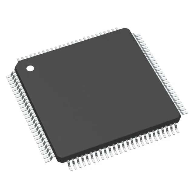
Renesas Electronics R7F7017643AFP-C#BA1 — Microcontrollers & Processors (MCU / MPU / DSP)

R7F7017643AFP-C#BA1 Renesas RH850/F1KM-S2 MCU, 240MHz

MPNR7F7017643AFP-C#BA1
End of Life

Renesas Electronics RH850/F1KM-S2 32-bit MCU, R7F7017643AFP-C#BA1, 240MHz RH850G3KH core, 2MB Flash, 256KB RAM, 128KB EEPROM, 100-LQFP.

$21.5Ref. price · indicative, final on quote
Packaging100-LQFP
StockIn Stock (22)
Lead timeIn Stock wk
MOQ1 pcs
  • 100% new & originalTraceable channels only — no refurbs, no pulls, no remarked parts.
  • Date & lot codes on quoteStated per line before you commit; label photos on request.
  • MSL-compliant ESD packingMoisture-sealed bags with indicator cards; reels photo-verified.
  • PayPal buyer protectionPay by T/T, PayPal or Payoneer — card payments covered end to end.

Specifications

R7F7017643AFP-C#BA1 Technical Specifications
ParameterValue
SeriesRH850/F1KM-S2
Mounting typeSurface Mount
Oscillator typeInternal
Program memory typeFLASH
Voltage - supply (Vcc (Vdd))3V ~ 5.5V
Operating temperature-40°C ~ 105°C (TA)
Speed240MHz
PackageTray
RAM size256K x 8
Core size32-Bit
EEPROM size128K x 8
PeripheralsDMA, PWM, WDT
ConnectivityCANbus, CSI, I²C, LINbus, SPI, UART/USART
Number of i (O)144
Core processorRH850G3KH
Case100-LQFP
Data convertersA/D 38x10b, 32x12b
Program memory size2MB (2M x 8)

Product details

240 MHz G3KH core with 2 MB on-chip flash

The R7F7017643AFP-C#BA1: The RH850G3KH core runs at 240 MHz, placing this MCU in the high-throughput tier for real-time control loops — a domain controller reading multiple CAN buses and executing torque-vectoring or transmission logic needs the clock headroom above 200 MHz to close the loop within a single 5 ms task cycle. 2 MB of program flash (2M x 8) with 256K x 8 RAM and 128K x 8 EEPROM-on-chip means the application image, data stacks, and calibration tables all fit without external memory — the EEPROM block is sized for fault-log storage and adaptive parameters over the vehicle lifetime.

Peripheral integration for body and domain control

Connectivity includes CANbus, CSI, I²C, LINbus, SPI, and UART/USART — the CAN and LIN interfaces directly match the automotive backbone, while CSI and SPI handle local sensor clusters and actuator drivers. 144 I/O pins give headroom for multiplexed switch inputs and LED diagnostics. The ADC bank offers 38 channels at 10-bit and 32 channels at 12-bit — the 12-bit group is the one to budget for analog sensors (throttle position, pressure, temperature) where 10 mV resolution on a 5 V reference is the difference between a valid reading and noise. On-chip peripherals include DMA, PWM, and WDT — the DMA engine offloads the core during high-rate CAN reception, and the PWM timers drive solenoid or H-bridge outputs directly without external pulse-generation logic.

Supply and temperature envelope for automotive duty

Operating temperature is -40°C to 105°C ambient — this is the under-hood / engine-bay band. A transmission ECU or engine controller sitting near the block sees 105°C on a summer-grade thermal profile; the 105°C rating leaves margin above the 85°C industrial limit.

The tray packaging is standard for automated pick-and-place; no moisture-sensitive bake is required if the floor-life limit is observed.

ROHS3 compliant.

Frequently asked questions

What is the closest functional alternative to R7F7017643AFP-C#BA1?

The R5F56604DDFP#30 from the RX600 series runs a 120 MHz RXv3 core, which is half the clock speed of the 240 MHz RH850G3KH here. The peripheral set overlaps (CANbus, I²C, LINbus, SPI), but the R5F56604DDFP#30 has 89 I/O versus 144, and its program memory is FLASH without the 128 KB EEPROM block. A board designed for the R7F7017643AFP-C#BA1 will not accept the R5F56604DDFP#30 without a PCB spin — different package and pinout.

What compliance documentation does Renesas provide for R7F7017643AFP-C#BA1?

ROHS3 compliant per the lifecycle entry.