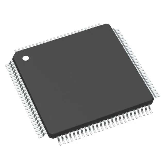
Renesas Electronics R7F100GPG3CFB#AA0 — Microcontrollers & Processors (MCU / MPU / DSP)

Renesas R7F100GPG3CFB#AA0 RL78/G23 MCU, 32 MHz, 128 KB Flash

MPNR7F100GPG3CFB#AA0
End of Life

Renesas Electronics RL78/G23 16-Bit Microcontroller, R7F100GPG3CFB#AA0, 32 MHz, 128 KB Flash, 16 KB RAM, 8 KB EEPROM, 88 I/O, 100-LQFP, -40 to 105°C.

$3.26Ref. price · indicative, final on quote
Packaging100-LQFP
StockIn Stock (20)
Lead timeIn Stock wk
MOQ1 pcs
  • 100% new & originalTraceable channels only — no refurbs, no pulls, no remarked parts.
  • Date & lot codes on quoteStated per line before you commit; label photos on request.
  • MSL-compliant ESD packingMoisture-sealed bags with indicator cards; reels photo-verified.
  • PayPal buyer protectionPay by T/T, PayPal or Payoneer — card payments covered end to end.

Specifications

R7F100GPG3CFB#AA0 Technical Specifications
ParameterValue
SeriesRL78/G23
Mounting typeSurface Mount
Oscillator typeInternal
Program memory typeFLASH
Voltage - supply (Vcc (Vdd))1.8V ~ 5.5V
Operating temperature-40°C ~ 105°C (TA)
Speed32MHz
PackageTray
RAM size16K x 8
Core size16-Bit
EEPROM size8K x 8
PeripheralsCapacitive Touch, LVD, POR, PWM, WDT
ConnectivityCSI, I²C, LINbus, SPI, UART/USART
Number of i (O)88
Core processorRL78
Case100-LQFP
Data convertersA/D 20x10b, 8x12b; D/A 2x8b
Program memory size128KB (128K x 8)

Product details

Flash and RAM budget — what fits before the linker cries

The R7F100GPG3CFB#AA0: 128 KB flash (128K x 8) holds the application code, the RL78/G23 HAL, and the bootloader without squeezing. The 16 KB RAM (16K x 8) is the tight spot — a full TCP/IP stack with a 1.5 KB MTU buffer leaves about 6 KB for the application heap and stack. Plan the linker sections so the.bss and.data fit within the 16 KB ceiling; the data flash EEPROM (8 KB) is separate and does not consume RAM. The 8 KB data flash is wear-leveled by the RL78/G23 hardware — no software wear-leveling needed for up to 100,000 write cycles per sector. Calibration constants, boot counters, and production serial numbers live here without an external EEPROM.

Supply rail and temperature — one rail from a Li-ion to a 5 V bus

A 100 nF ceramic at each VDD pin plus a 10 µF bulk cap on the main rail is the standard decoupling; the 100-LQFP has 12 power/ground pins, so the IR drop across the package is low.

Peripheral mux and I/O count — 88 pins that can be anything

88 I/O pins in the 100-LQFP — the remaining 12 pins are power, ground, and the reset line. The RL78/G23 serial array unit (SAU) lets you map CSI, I²C, LINbus, SPI, or UART/USART to any of the general-purpose I/O pins; there is no fixed peripheral pin assignment. The capacitive touch unit runs independently of the CPU and supports up to 36 channels — no external touch controller for a membrane keypad. The 20-channel 10-bit ADC scans fast at up to 1 MHz conversion rate; the 8-channel 12-bit ADC delivers 1 LSB INL for precision analog inputs like thermistor bridges or current-sense amplifiers. The 2-channel 8-bit DAC outputs a reference voltage or an analog signal for external sensor excitation.

Frequently asked questions

What is the closest pin-compatible alternative to R7F100GPG3CFB#AA0 in the RL78/G23 family?

The RL78/G23 family shares the same 100-LQFP footprint across multiple flash and RAM options. A pin-compatible alternative with larger memory is the R7F100GPG4CFB#AA0 (256 KB flash, 24 KB RAM). Confirm the exact memory and peripheral requirements before substituting.

What compliance documentation does Renesas provide for R7F100GPG3CFB#AA0?

Renesas provides a RoHS3 compliance certificate and the standard REACH declaration for the RL78/G23 series. The datasheet includes the material composition declaration. No UL or IEC certification is listed for this microcontroller — it is a commercial/industrial IC, not a safety-rated component.