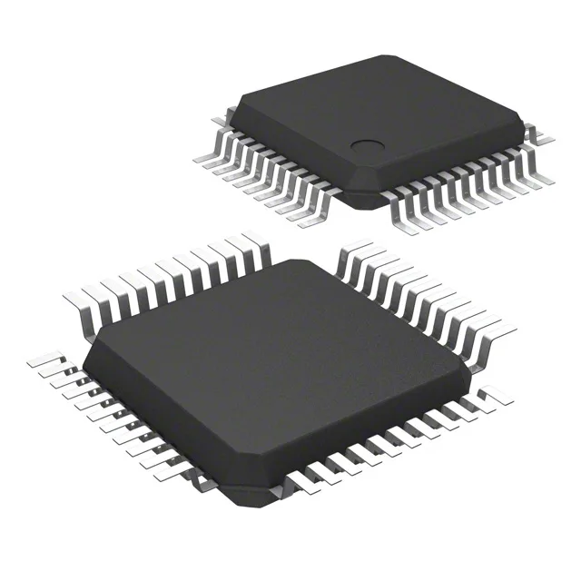
Active RL78/G23 MCU with 32 MHz core and 192 KB Flash
The R7F100GFH3CFP#HA0: The 32 MHz core speed sets the instruction throughput ceiling; the 16-bit RL78 architecture executes most instructions in 1-2 clock cycles, so the effective MIPS rate is close to the clock frequency for register-to-register operations.
Memory and data retention
The 192 KB Flash is organised as 192K x 8 bits, suitable for application code and bootloader storage. The 8 KB EEPROM is separate from the program Flash, so data logging parameters and calibration constants survive firmware updates without sector-erase overhead. 20 KB of RAM provides stack and heap headroom for moderate-sized control loops and communication buffers. For a typical sensor-fusion application with 4 KB of global variables and a 2 KB RTOS kernel, the remaining 14 KB is available for dynamic allocation.
Analog and peripheral integration
The ADC block offers 10 channels with selectable 8-bit, 10-bit, or 12-bit resolution. The 12-bit mode delivers 4096 counts across the reference voltage; the 8-bit mode is useful for fast oversampling or when the sensor noise floor exceeds the LSB size. Two 8-bit DAC channels can generate analog setpoints or bias voltages without external DACs. On-chip peripherals include capacitive touch sensing, low-voltage detect (LVD), power-on reset (POR), PWM, and watchdog timer. The capacitive touch block supports up to 36 self-capacitance channels and 144 mutual-capacitance channels — enough for a membrane keypad or slider without an external touch controller.
Connectivity and package
Serial interfaces include CSI (clocked serial interface), I²C, LINbus, SPI, and UART/USART. The 44-LQFP package has a 10x10 mm body with 0.8 mm pitch — routable on a 2-layer board with standard trace widths. 37 general-purpose I/O pins are available; the remaining pins are dedicated to power, ground, and oscillator.