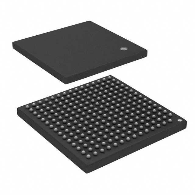
Renesas Electronics R5F572MDDGBD#20 — Microcontrollers & Processors (MCU / MPU / DSP)

Renesas R5F572MDDGBD#20 RX MCU, 240 MHz, 2 MB Flash

MPNR5F572MDDGBD#20
End of Life

Renesas Electronics RX series 32-bit MCU, RXv3 core, 240 MHz, 2 MB FLASH, 1 MB RAM, 182 I/O, 224-LFBGA (13x13), -40°C to +105°C.

$18.04Ref. price · indicative, final on quote
Packaging224-LFBGA
StockContact for availability
Lead timeIn Stock wk
MOQ1 pcs
  • 100% new & originalTraceable channels only — no refurbs, no pulls, no remarked parts.
  • Date & lot codes on quoteStated per line before you commit; label photos on request.
  • MSL-compliant ESD packingMoisture-sealed bags with indicator cards; reels photo-verified.
  • PayPal buyer protectionPay by T/T, PayPal or Payoneer — card payments covered end to end.

Specifications

R5F572MDDGBD#20 Technical Specifications
ParameterValue
SeriesRX
Mounting typeSurface Mount
Oscillator typeInternal
Program memory typeFLASH
Voltage - supply (Vcc (Vdd))2.7V ~ 3.6V
Operating temperature-40°C ~ 105°C (TA)
Speed240MHz
PackageTray
RAM size1M x 8
Core size32-Bit
EEPROM size32K x 8
PeripheralsDMA, LCD, LVD, POR, PWM, WDT
ConnectivityCANbus, EBI/EMI, Ethernet, I²C, MMC/SD, QSPI, SCI, SPI, SSI, USB OTG
Number of i (O)182
Core processorRXv3
Case224-LFBGA
Data convertersA/D 29x12b; D/A 2x12b
Program memory size2MB (2M x 8)

Product details

240 MHz RXv3 core with 2 MB flash — industrial control headroom

The R5F572MDDGBD#20 is a Renesas RX-series 32-bit microcontroller built around the RXv3 core running at 240 MHz. That clock speed, combined with 2 MB of on-chip flash and 1 MB of SRAM, gives it the throughput and memory footprint to run a real-time control loop, a communication stack, and a local data buffer without reaching for external memory. The 32 KB EEPROM block is useful for storing calibration constants, node IDs, or fault logs that survive a firmware update — no separate serial EEPROM needed on the board.

Peripheral set for gateway and motion-control designs

Connectivity includes Ethernet, CAN, USB OTG, QSPI, I²C, SPI, SCI, SSI, and MMC/SD — enough to serve as a fieldbus gateway aggregating sensor data over CAN or Ethernet and logging it to an SD card. The 182 general-purpose I/O in the 224-LFBGA package allow parallel bus interfaces to FPGAs or external ADCs without muxing.

Active lifecycle — no LTB clock ticking

RoHS3 compliant per the manufacturer's declaration.