240 MHz RXv3 core with 2 MB Flash — where the headroom lands
The R5F572MDDDFP#10 runs a 32-bit RXv3 core at 240 MHz, with 2 MB of Flash program memory and 1 MB of SRAM on-chip. That Flash-to-SRAM ratio — 2:1 — means the code footprint for a real-time control stack with Ethernet and CAN stacks fits without external memory, and the 1 MB SRAM handles multiple frame buffers or a large data logger without paging. The 32 KB EEPROM is a separate non-volatile block for calibration constants or boot parameters that survive reprogramming of the main Flash — useful for field-updatable firmware that must keep its configuration across an erase cycle.
Peripheral mix — Ethernet, CAN, USB OTG, and storage interfaces on one die
Connectivity includes Ethernet, CANbus, USB OTG, I²C, SPI, QSPI, SCI (UART), SSI, and MMC/SD — enough to serve as the application processor in a programmable logic controller (PLC) or an industrial gateway that bridges fieldbus to Ethernet. The EBI/EMI bus can interface to external SRAM, NOR Flash, or an FPGA without a glue-logic CPLD. The 29-channel 12-bit ADC and 2-channel 12-bit DAC cover analog sensor acquisition and setpoint output for motor-drive or process-control loops.
Industrial temperature grade and package — board-fit constraints
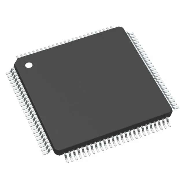
The 100-LQFP package (14×14 mm body) has a 0.50 mm pitch — a 4-layer board is recommended for fan-out of the peripheral signals, especially the Ethernet and USB differential pairs. The 72 general-purpose I/O pins are 3.3 V tolerant; level translation is needed only for legacy 5 V peripherals.