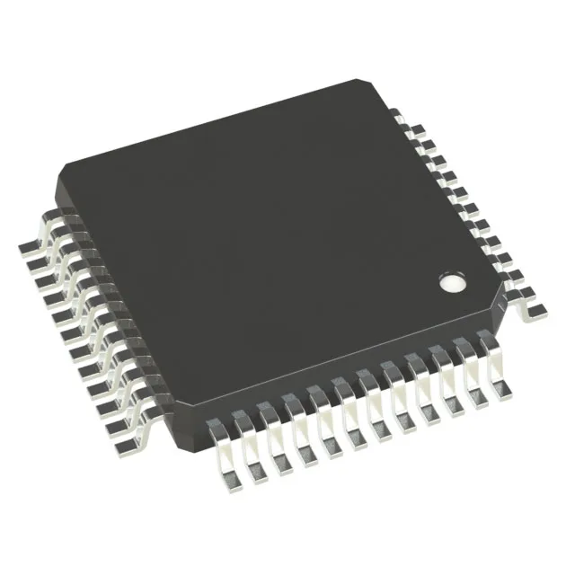
Renesas Electronics R5F566TEBGFL#10 — Microcontrollers & Processors (MCU / MPU / DSP)

R5F566TEBGFL#10 Renesas RXv3 MCU, 160MHz, 512KB Flash

MPNR5F566TEBGFL#10
End of Life

Renesas Electronics RX series RXv3 32-bit MCU, R5F566TEBGFL#10, 160 MHz, 512 KB Flash, 64 KB RAM, 32 KB EEPROM, 48-LQFP, Tray.

$5.73Ref. price · indicative, final on quote
Packaging48-LQFP
StockIn Stock (28)
Lead timeIn Stock wk
MOQ1 pcs
  • 100% new & originalTraceable channels only — no refurbs, no pulls, no remarked parts.
  • Date & lot codes on quoteStated per line before you commit; label photos on request.
  • MSL-compliant ESD packingMoisture-sealed bags with indicator cards; reels photo-verified.
  • PayPal buyer protectionPay by T/T, PayPal or Payoneer — card payments covered end to end.

Specifications

R5F566TEBGFL#10 Technical Specifications
ParameterValue
SeriesRX
Mounting typeSurface Mount
Oscillator typeInternal
Program memory typeFLASH
Voltage - supply (Vcc (Vdd))2.7V ~ 5.5V
Operating temperature-40°C ~ 105°C (TA)
Speed160MHz
PackageTray
RAM size64K x 8
Core size32-Bit
EEPROM size32K x 8
PeripheralsDMA, LVD, POR, PWM, WDT
ConnectivityCANbus, EBI/EMI, I²C, LINbus, MMC/SD, SCI, SPI, SSI, UART/USART
Number of i (O)33
Core processorRXv3
Case48-LQFP
Data convertersA/D 8x12b; D/A 2x12b
Program memory size512KB (512K x 8)

Product details

Core compute and memory budget

The R5F566TEBGFL#10 runs the RXv3 core at 160 MHz — the instruction pipeline and flash prefetch buffer are tuned so that most single-cycle instructions execute at that clock without wait states for cached code. The 512 KB on-chip flash and 64 KB SRAM leave room for a real-time OS kernel, a moderate application stack, and a communication buffer for CAN or Ethernet frames. A separate 32 KB EEPROM block handles parameter storage and calibration data without wearing the main flash — useful for field-updatable firmware where the EEPROM endurance (typically 1M cycles) outlasts the flash sector erase cycles.

Peripheral set and analog integration

The part integrates eight 12-bit ADC channels and two 12-bit DAC channels — enough for a three-phase motor current-sense plus a reference voltage output, all on a single 48-pin LQFP. The DMA controller can shuttle ADC results directly to RAM without CPU intervention, keeping the core free for control loops. Connectivity covers CANbus, I²C, SPI, SCI (UART), LINbus, and an EBI/EMI bus for external memory or FPGA glue logic. The MMC/SD interface supports data logging to an SD card without an external controller. Built-in LVD (low-voltage detect) and POR (power-on reset) eliminate the need for an external supervisor IC in most designs — the MCU holds the reset line until the supply rail is stable above the threshold.

Sourcing and lifecycle posture

The part is ROHS3 compliant.

Frequently asked questions

Will R5F566TEBGFL#10 drop into a board designed for R5F566TEBDFL#10?

The two parts share the same 48-LQFP package, core, memory size, and peripheral set. If the board's thermal environment stays below 85°C, the BOM can accept either order code without a board spin.

What compliance documentation is available for R5F566TEBGFL#10?

Renesas provides ROHS3 compliance certification. No UL, IEC, or REACH documentation is listed in the product record — confirm with the factory or distributor at RFQ if a specific regulatory filing is required.