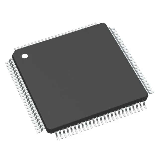
Renesas Electronics R5F56609ADFP#30 — Microcontrollers & Processors (MCU / MPU / DSP)

R5F56609ADFP#30 Renesas RX600 MCU, 120MHz, 1MB Flash

MPNR5F56609ADFP#30
End of Life

Renesas Electronics RX600 series 32-Bit MCU, RXv3 core, 120MHz, 1MB Flash, 128K x 8 RAM, 32K x 8 EEPROM, 100-LQFP, Tray.

$6.7Ref. price · indicative, final on quote
Packaging100-LQFP
StockContact for availability
MOQ1 pcs
  • 100% new & originalTraceable channels only — no refurbs, no pulls, no remarked parts.
  • Date & lot codes on quoteStated per line before you commit; label photos on request.
  • MSL-compliant ESD packingMoisture-sealed bags with indicator cards; reels photo-verified.
  • PayPal buyer protectionPay by T/T, PayPal or Payoneer — card payments covered end to end.

Specifications

R5F56609ADFP#30 Technical Specifications
ParameterValue
SeriesRX600
Mounting typeSurface Mount
Oscillator typeExternal, Internal
Program memory typeFLASH
Voltage - supply (Vcc (Vdd))2.7V ~ 5.5V
Operating temperature-40°C ~ 85°C (TA)
Speed120MHz
PackageTray
RAM size128K x 8
Core size32-Bit
EEPROM size32K x 8
PeripheralsDMA, LVD, POR, PWM, WDT
ConnectivityCANbus, EBI/EMI, I²C, LINbus, SCI, SPI
Number of i (O)91
Core processorRXv3
Case100-LQFP
Data convertersA/D 24x12b; D/A 2x12b
Program memory size1MB (1M x 8)

Product details

120 MHz RXv3 core with 1 MB on-chip flash

The R5F56609ADFP#30 is a 32-bit microcontroller from the Renesas RX600 series, built around the RXv3 core running at 120 MHz. This puts its throughput ceiling above what a 100 MHz Cortex-M4 can sustain on a single-cycle multiply-accumulate loop — relevant for motor-field-oriented control or a multi-axis servo interpolator where the control-law update rate is the bottleneck. Program memory is 1 MB of flash, backed by 128 KB of SRAM and a separate 32 KB EEPROM block. The EEPROM is a dedicated array, not emulated flash — it handles byte-level writes without erase cycles, so a data logger writing configuration parameters every power cycle does not wear the main program flash.

Peripheral set for a single-chip control node

The 91 I/O lines in the 100-LQFP package mean most of the port pins are brought out; a parallel LCD bus or a bank of discrete opto-inputs can be wired without a port expander. On the connectivity side: CAN, I2C, SPI, SCI (UART), and LINbus cover the common fieldbus and sensor interfaces in an industrial drive or PLC I/O module. The external bus interface (EBI/EMI) lets you map an external SRAM or FPGA register file into the memory space without bit-banging GPIO. The wide tolerance means a lightly regulated 5 V bus from a cheap wall wart still keeps the core inside spec, and the 5 V-tolerant I/O eliminates level shifters on the sensor inputs.

Industrial temperature grade and active lifecycle

ROHS3 compliant — no exemptions for lead in solder or PBB/PBDE flame retardants. The 100-LFQFP package has a 14x14 mm body with 0.50 mm pitch; the exposed pad is on the bottom, not the sides, so a standard QFP solder profile and X-ray inspection catch the joints.

Frequently asked questions

What is the closest functional alternative to R5F56609ADFP#30?

The peer R5F56609DDFP#30 shares the same RXv3 core at 120 MHz, the same 1 MB flash, 128 KB RAM, 32 KB EEPROM, and the same peripheral set including 24x12b ADC and dual DAC. The difference is 89 I/O instead of 91 — two fewer port pins — in the same 100-LQFP footprint. It drops into the same board layout and BOM position without a PCB spin.