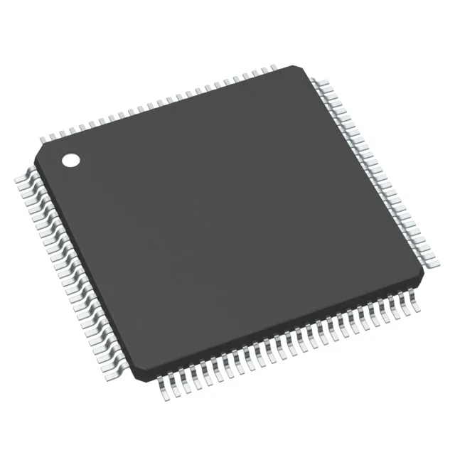
Renesas Electronics R5F565N7BGFP#30 — Microcontrollers & Processors (MCU / MPU / DSP)

R5F565N7BGFP#30 Renesas RX65N MCU, 120MHz, 768KB Flash

MPNR5F565N7BGFP#30
End of Life

Renesas Electronics RX65N 32-bit MCU, R5F565N7BGFP#30, 120MHz RXv2 core, 768KB Flash, 256KB RAM, 100-LQFP, -40 to +105°C, Ethernet, CAN, USB.

$7.49Ref. price · indicative, final on quote
Packaging100-LQFP
StockIn Stock (23)
Lead timeIn Stock wk
MOQ1 pcs
  • 100% new & originalTraceable channels only — no refurbs, no pulls, no remarked parts.
  • Date & lot codes on quoteStated per line before you commit; label photos on request.
  • MSL-compliant ESD packingMoisture-sealed bags with indicator cards; reels photo-verified.
  • PayPal buyer protectionPay by T/T, PayPal or Payoneer — card payments covered end to end.

Specifications

R5F565N7BGFP#30 Technical Specifications
ParameterValue
SeriesRX65N
Mounting typeSurface Mount
Oscillator typeExternal
Program memory typeFLASH
Voltage - supply (Vcc (Vdd))2.7V ~ 3.6V
Operating temperature-40°C ~ 105°C (TA)
Speed120MHz
PackageTray
RAM size256K x 8
Core size32-Bit
PeripheralsDMA, LVD, POR, PWM, WDT
ConnectivityCANbus, EBI/EMI, Ethernet, I²C, LINbus, MMC/SD, QSPI, SCI, SPI, UART/USART, USB
Number of i (O)78
Core processorRXv2
Case100-LQFP
Data convertersA/D 22x12b; D/A 1x12b
Program memory size768KB (768K x 8)

Product details

120 MHz RXv2 core with 768 KB flash — single-chip control for industrial gateways

The R5F565N7BGFP#30 is a Renesas RX65N series 32-bit microcontroller built around the RXv2 core running at 120 MHz. With 768 KB of on-chip flash and 256 KB of RAM, it holds both the application firmware and a real-time data buffer without external memory for many control-loop and gateway designs. The 100-LQFP package (14x14 mm body) provides 78 accessible GPIOs — enough to interface a parallel LCD, external memory bus, and multiple serial peripherals while leaving headroom for panel buttons and status LEDs.

Ethernet, CAN, USB, QSPI — the connectivity set for a fieldbus gateway node

On-chip Ethernet MAC, CAN 2.0B, USB 2.0 full-speed, and a Quad SPI interface let this MCU bridge between a factory EtherNet/IP or Modbus TCP backbone and local sensor/actuator buses over I²C, SPI, or UART. The EBI/EMI interface can also connect an external SRAM or NOR flash for data logging beyond the internal 256 KB. The 22-channel 12-bit ADC samples analog inputs from thermocouples, pressure transducers, or current shunts; the single 12-bit DAC outputs an analog setpoint or reference voltage.

-40 to +105°C industrial temperature grade — motor-drive and outdoor deployment

The part is ROHS3 compliant and supplied in tray packaging.

Frequently asked questions

What is the maximum clock speed of the R5F565N7BGFP#30?

The RXv2 core runs at 120 MHz. This is the CPU clock ceiling; the flash wait-state controller must be configured to match the cycle time for zero-wait access at that frequency.

What package does the R5F565N7BGFP#30 come in?

The supplier device package is also listed as 100-LFQFP (14x14). Both refer to the same footprint.

What serial interfaces are available on this MCU?

The device includes Ethernet MAC, CAN 2.0B, USB 2.0 full-speed, QSPI, I²C, SCI (UART), SPI, and LINbus.

How do I get current pricing and availability for the R5F565N7BGFP#30?

Submit an RFQ through this listing.