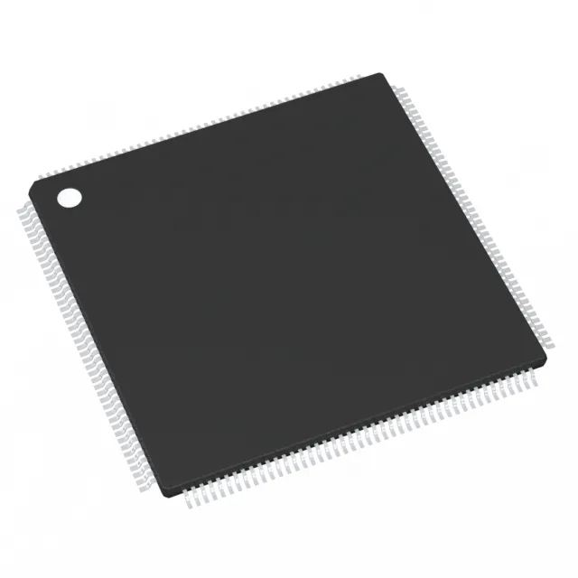
RXv2 core at 120 MHz — throughput for real-time control stacks
The R5F565N4BGFB#30 is a 32-bit RX65N series MCU built around the RXv2 core, clocked at 120 MHz. That clock rate, combined with the DMA engine and the on-chip 256 KB RAM, gives it the headroom to run a real-time OS, a TCP/IP stack, and a fieldbus protocol without starving the control loop.
On-chip memory budget — 512 KB flash, 256 KB RAM
Program memory is 512 KB of flash, with 256 KB of SRAM. That RAM allocation is enough to buffer two full Ethernet frames (1536 bytes each) plus a CAN message queue and still leave room for the application heap. The flash size supports a full Renesas FSP or Azure RTOS footprint with room for a modest application image.
Wired connectivity without an external bridge
The peripheral set includes Ethernet MAC, dual CAN 2.0B channels, USB 2.0 Full Speed, and multiple SCI/SPI/I²C serial interfaces. That means a single MCU handles the three most common industrial fieldbuses — EtherNet/IP, CANopen, and Modbus RTU — without an external communication coprocessor. The 111 general-purpose I/O pins, combined with the EBI/EMI bus, allow direct connection to external SRAM, NOR flash, or an FPGA over a parallel memory interface without glue logic.
Analog front-end — 29-channel ADC, dual DAC
The 12-bit ADC scans 29 channels — enough to monitor three-phase motor currents, DC bus voltage, and four temperature sensors in a single conversion sequence. The dual 12-bit DAC can generate analog setpoints or bias voltages without an external converter.
The -40 to +105 °C operating range covers the industrial ambient band with margin for self-heating. Supply voltage is 2.7 to 3.6 V, compatible with a single 3.3 V rail.
Active lifecycle — no end-of-life signal
ROHS3 compliant.