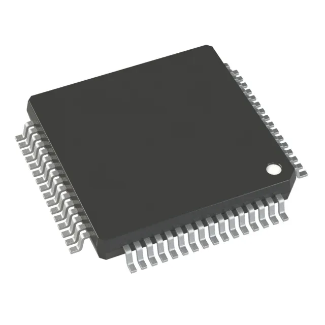
RXv2 core at 48 MHz — throughput and memory partition
The R5F51406AGFM#30 runs the RXv2 core at 48 MHz, a 32-bit single-core architecture with a single-cycle multiply and hardware divider. For a typical sensor-fusion loop reading 15 ADC channels and updating a PWM output, the 48 MHz ceiling leaves margin for the control algorithm without needing to optimize in assembly. On-chip memory breaks down as 256 KB flash for firmware and calibration tables, 64 KB SRAM for stack and data buffers, and 8 KB dedicated EEPROM — the EEPROM is separate from the flash array, so wear-leveling logic for parameter storage is optional rather than mandatory. A firmware image with a 50 KB HAL + 30 KB application stack leaves about 170 KB free for application code and lookup tables.
Supply rail and temperature — single-voltage industrial operation
The 1.8 V floor allows battery-powered designs to drain the cell deeper before the BOD trips. The internal oscillator is trimmed across this range; for a CANbus node on a factory floor that sees 85 °C in summer, the clock drift stays within the CAN bit-timing budget without an external crystal.
Package and board integration — 64-LQFP with 53 usable GPIO
The 0.5 mm pitch demands a 4-layer PCB for reliable fan-out of the inner rows; a 2-layer board can break out only the perimeter pins without via-in-pad. No exposed thermal pad — the LFQFP variant relies on the leadframe for heat conduction.
Analog and peripheral complement — ADC, DAC, capacitive touch, CAN
The ADC subsystem provides 15 channels of 12-bit resolution — enough to sample three three-phase current sensors plus a DC-link voltage and a temperature NTC without an external analog mux. The two 8-bit DAC channels can generate analog setpoints or bias voltages for external op-amps. On-chip peripherals include capacitive touch sensing (self- and mutual-capacitance), a CANbus controller, three SCI (UART) channels, two I²C, and one SPI. The DMA controller can move ADC results directly to RAM without CPU intervention — useful for a motor-control loop that samples current at 10 kHz and updates PWM every 100 µs.
The ROHS3 compliance covers all ten restricted substances with no exemptions, so it passes EU RoHS for finished goods shipped into Europe.