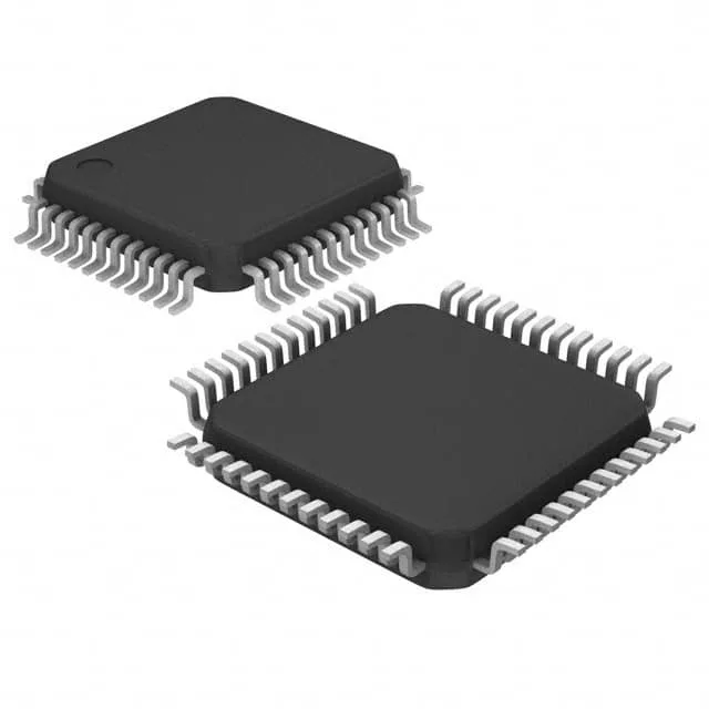
Renesas Electronics R5F51403AGNE#30 — Microcontrollers & Processors (MCU / MPU / DSP)

R5F51403AGNE#30 RX140 MCU, 48 MHz, 64 KB Flash, 48-HWQFN

MPNR5F51403AGNE#30
End of Life

Renesas RX140 series 32-bit MCU, R5F51403AGNE#30, 48 MHz RX core, 64 KB flash, 16 KB RAM, 4 KB EEPROM, 39 I/O, 11x12-bit ADC, -40 to 105°C, 48-HWQFN.

$2.76Ref. price · indicative, final on quote
Packaging48-WFQFN Exposed Pad
StockIn Stock (19)
Lead timeIn Stock wk
MOQ1 pcs
  • 100% new & originalTraceable channels only — no refurbs, no pulls, no remarked parts.
  • Date & lot codes on quoteStated per line before you commit; label photos on request.
  • MSL-compliant ESD packingMoisture-sealed bags with indicator cards; reels photo-verified.
  • PayPal buyer protectionPay by T/T, PayPal or Payoneer — card payments covered end to end.

Specifications

R5F51403AGNE#30 Technical Specifications
ParameterValue
SeriesRX140
Mounting typeSurface Mount
Oscillator typeInternal
Program memory typeFLASH
Voltage - supply (Vcc (Vdd))1.8V ~ 5.5V
Operating temperature-40°C ~ 105°C (TA)
Speed48MHz
PackageTray
RAM size16K x 8
Core size32-Bit Single-Core
EEPROM size4K x 8
PeripheralsDMA, LVD, POR, PWM, WDT
ConnectivityI²C, SCI, SPI
Number of i (O)39
Core processorRX
Case48-WFQFN Exposed Pad
Data convertersA/D 11x12b
Program memory size64KB (64K x 8)

Product details

48 MHz RX core in a 7x7 mm QFN

The R5F51403AGNE#30 is a 32-bit single-core RX microcontroller from the RX140 series, clocked at 48 MHz. It packs 64 KB of flash and 16 KB of RAM into a 48-HWQFN package with a 7x7 mm footprint and an exposed thermal pad. The 48 MHz clock is the ceiling for instruction-fetch cycles from flash; the RX core's single-cycle multiply-accumulate unit keeps real-time control loops deterministic without wait-state jitter at that speed.

Supply, temperature, and board integration

The 48-HWQFN package requires a thermal-via array under the exposed pad to pull heat into the ground plane. The 0.5 mm pitch demands a four-layer board for reliable fan-out of the 39 I/O — two-layer break-out is possible but risks signal-integrity issues on the outer rows.

On-chip peripherals and sensor interface

Eleven 12-bit ADC channels give this part enough analog front-end for a three-phase motor current-sense plus a thermistor or two, all sampled sequentially through the scan list. The DMA controller can shuttle conversion results to RAM without CPU intervention — the core stays free for the control loop. Serial connectivity covers I²C, SCI (UART), and SPI — enough to talk to an external EEPROM, a hall-effect current sensor over SPI, and a Modbus RTU link over SCI simultaneously. The 4 KB of data flash (EEPROM emulation) stores calibration coefficients and fault logs with 100,000 write-cycle endurance.

Frequently asked questions

What is the closest pin-compatible alternative to R5F51403AGNE#30 in the RX140 family?

The RX140 series includes variants with larger flash (up to 128 KB) and more I/O, but they use different package pinouts. A board layout change is required for a different flash-size variant.

What compliance documentation does Renesas provide for R5F51403AGNE#30?

The part is ROHS3 compliant. Renesas publishes a material declaration and REACH compliance statement for the RX140 series through their standard documentation portal.