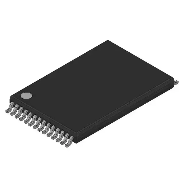
Active 256Kbit parallel SRAM for embedded data buffering
The Renesas R1LV5256ESA-7SI#B0 is a 256 Kbit volatile SRAM organized as 32K x 8 bits, accessed through a parallel interface. With a 70 ns access time and matching 70 ns write cycle (word/page), this part is suited for microcontroller and FPGA applications where the memory controller needs a deterministic, moderate-speed SRAM for scratchpad, frame buffers, or cache expansion.
70 ns speed grade — timing margin for the bus
The 70 ns access time and 70 ns write cycle define the window the memory controller has to assert addresses, strobe the chip, and read or write data. In a system with a 10 MHz bus clock (100 ns period), this leaves 30 ns of margin for PCB trace delay and controller setup/hold — workable for a single-load bus but tight if multiple SRAMs share the same address/control lines. At the cold end, access time typically improves; at 85°C, the part may slow by 10-15% from the 25°C typical, but the 70 ns max is specified across the full range.
28-TSOP footprint and supply flexibility
Housed in a 28-TSSOP package (0.465-inch body width, 11.80 mm), the part is also described with the supplier device package as 28-TSOP. Below 2.7 V the SRAM data is not guaranteed; a brown-out detector should hold the chip in deselect or trigger a reset.
Active lifecycle — no end-of-life pressure
No official successor or second-source part number is recorded in the Renesas documentation.