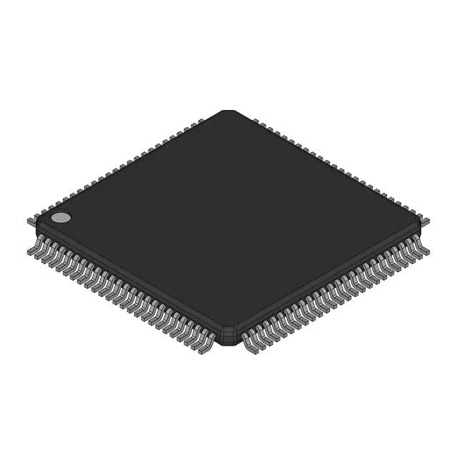
Renesas Electronics 71V3558S100PFGI — DC-DC Power Modules

71V3558S100PFGI SRAM, 4.5Mbit 100 MHz Synchronous ZBT

MPN71V3558S100PFGI
End of Life

Renesas 71V3558S100PFGI, 4.5Mbit Synchronous SRAM (ZBT), 100 MHz clock, 5 ns access time, 256K x 18 organization, Parallel interface, 3.135V–3.465V supply, -40°C to 85°C, 100-TQFP (14x14).

$5.93Ref. price · indicative, final on quote
Packaging100-LQFP
Independent supplier — new & surplus stockAuthenticity-screened · ESD-safe packingListing updated Jul 2026

Specifications

71V3558S100PFGI specifications
ParameterValue
Memory typeVolatile
MountingSurface Mount
Voltage3.135V ~ 3.465V
Frequency100 MHz
Memory interfaceParallel
Operating temperature-40°C ~ 85°C (TA)
PackageBulk
TechnologySRAM - Synchronous, SDR (ZBT)
Access time5 ns
Memory size4.5Mbit
Memory formatSRAM
Case100-LQFP
Memory organization256K x 18

Product details

100 MHz synchronous ZBT SRAM for high-throughput data paths

The Renesas 71V3558S100PFGI is a 4.5 Mbit synchronous SRAM built on a Zero Bus Turnaround (ZBT) architecture, clocked at 100 MHz with a 5 ns access time. It is organized as 256K words of 18 bits each, accessed through a parallel interface. This part targets applications where the memory bus must sustain back-to-back reads and writes without dead cycles — think network packet buffers, DSP scratchpads, and high-speed cache in telecom line cards or industrial controllers.

5 ns access time and 100 MHz clock — what they mean for bus timing

The 5 ns access time is the time from address assertion to valid data on the outputs. At a 100 MHz clock (10 ns period), that leaves roughly 5 ns of setup margin for the controller to latch the data — tight enough that signal-integrity on the address and data buses matters. The ZBT pipeline eliminates the turnaround cycle between read and write, so the controller can alternate transactions every clock edge without inserting idle cycles. If your FPGA or ASIC memory controller expects a pipelined synchronous SRAM with a 100 MHz ceiling, this part fits the timing budget.

The supply range of 3.135 V to 3.465 V (3.3 V nominal ±5%) aligns with standard 3.3 V logic rails. If your system runs a 3.3 V bus with a ±5% regulator, this SRAM stays within spec across the full temperature range without needing a separate supply.

The active status also means franchised distribution channels carry it, so supply is available through standard procurement routes.

Frequently asked questions

Is 71V3558S100PFGI still in production or obsolete?

Buyers need lifecycle status to avoid redesign or last-time buy issues.

What is the access time and memory organization of 71V3558S100PFGI?

Design engineers verify timing compatibility and memory width.

Where can I buy 71V3558S100PFGI at the best price?

Sourcing buyers compare prices across distributors to minimize BOM cost.

What is the pinout and package footprint for 71V3558S100PFGI?

Layout engineers need pin mapping and land pattern for PCB design.

Is there a direct replacement or cross reference for 71V3558S100PFGI?

Maintenance techs and brokers need alternatives when part is unavailable or obsolete.

What is the typical lead time for 71V3558S100PFGI?

Buyers need delivery schedule to plan production and avoid shortages.