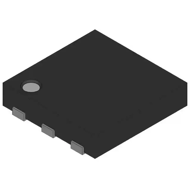
Dual-transistor BOM consolidation in a single 2x2 mm package
The PBSS4230PANP,115 packs both an NPN and a PNP transistor into one 6-HUSON (2x2) package, cutting the component count for push-pull drivers, H-bridge pre-drivers, and level translators. Each side handles 2 A continuous collector current with a 30 V Vce breakdown, so it drives small relays, solenoids, and logic-level loads directly from a 24 V supply rail. The 120 MHz transition frequency means it switches comfortably in the 100 kHz to 1 MHz range for DC-DC converter gate drive or Class-D audio pre-drive — the speed limit is set by the load capacitance and base drive, not the die itself.
Low saturation voltage and high gain reduce thermal stress
Vce(sat) is just 290 mV at 200 mA base current and 2 A collector current — conduction loss at 2 A is under 0.6 W, which the 510 mW package rating can handle only with the exposed pad soldered to a copper plane. Without the pad thermal path, the junction temperature climbs above the 150°C (TJ) limit at full load. DC current gain (hFE) is a minimum of 200 at 1 A collector current and 2 V Vce — this means a microcontroller GPIO sourcing just 5 mA can saturate the transistor at 1 A load, eliminating the need for a separate driver stage in low-side switching applications. Collector cutoff current is max 100 nA (ICBO) — negligible leakage in battery-powered circuits where the load is switched off for long periods.
Package footprint and reflow considerations
The 6-UFDFN Exposed Pad package (6-HUSON, 2x2 mm) has a 0.5 mm pitch — the centre pad must be soldered to a thermal via array under the part to pull heat into the inner copper layers. Without the via pattern, the 510 mW dissipation limit derates sharply above 25°C ambient. The Bulk packaging means parts arrive in tubes or trays, not tape-and-reel — plan for manual or tube-fed placement; no reel changeover on the pick-and-place line.
Active production — no end-of-life concerns for new designs
The 150°C (TJ) junction temperature rating aligns with industrial temperature environments — motor-drive enclosures, power-supply hot spots, and automotive under-hood zones where ambient hits 105°C still leave 45°C margin before the die limit.