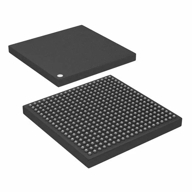
NXP Semiconductors MCIMX502CVM8B — Microcontrollers & Processors (MCU / MPU / DSP)

NXP MCIMX502CVM8B i.MX50 ARM Cortex-A8 800MHz MPU

MPNMCIMX502CVM8B
End of Life

NXP Semiconductors i.MX50 series ARM Cortex-A8 microprocessor, MCIMX502CVM8B, 800MHz, 400-LFBGA (17x17), USB 2.0 + PHY, 10/100 Ethernet, LCD controller.

$25.77Ref. price · indicative, final on quote
Packaging400-LFBGA
StockIn Stock (22)
Lead timeIn Stock wk
MOQ1 pcs
  • 100% new & originalTraceable channels only — no refurbs, no pulls, no remarked parts.
  • Date & lot codes on quoteStated per line before you commit; label photos on request.
  • MSL-compliant ESD packingMoisture-sealed bags with indicator cards; reels photo-verified.
  • PayPal buyer protectionPay by T/T, PayPal or Payoneer — card payments covered end to end.

Specifications

MCIMX502CVM8B Technical Specifications
ParameterValue
Seriesi.MX50
Mounting typeSurface Mount
Voltage - i (O)1.2V, 1.875V, 2.775V, 3.0V
Additional interfaces1-Wire, AC'97, I²C, I²S, MMC/SD, SPI, SSI, UART
Display & interface controllersLCD
Operating temperature0°C ~ 70°C (TA)
Number of cores (Bus width)1 Core, 32-Bit
USBUSB 2.0 + PHY (2)
Speed800MHz
PackageTray
Ethernet10/100Mbps (1)
Core processorARM® Cortex®-A8
Case400-LFBGA
RAM controllersLPDDR, LPDDR2, DDR2
Co-Processors (DSP)Multimedia; NEON™ SIMD
Security featuresBoot Security, Cryptography, Secure JTAG
Graphics accelerationYes

Product details

800 MHz Cortex-A8 with on-chip PHYs

The MCIMX502CVM8B is an i.MX50-series application processor built around a single ARM Cortex-A8 core clocked at 800 MHz, with a NEON SIMD media coprocessor for vector math acceleration. Two USB 2.0 interfaces with integrated PHY and a single 10/100 Mbps Ethernet MAC mean the BOM avoids external transceivers for wired connectivity — the Ethernet port still needs an external PHY chip, but the MAC layer is on-die. The memory controller supports LPDDR, LPDDR2, and DDR2, giving the layout engineer a choice between low-power mobile DRAM and commodity DDR2 depending on the cost and power budget.

Package, power rails, and temperature grade

The I/O voltage domain is split across four rails — 1.2 V, 1.875 V, 2.775 V, and 3.0 V — so the power tree must generate these separately; a common sequencing trap is assuming a single 3.3 V rail feeds all I/O banks.

Boot flow and security perimeter

The i.MX50 boots from internal ROM that probes the boot device order — MMC/SD, SPI NOR, NAND, or USB — configurable via the BOOT_MODE pins; the first-power checklist should verify the strap resistors before expecting a serial download. Hardware security features include boot-time cryptography, secure JTAG, and a cryptographic accelerator — useful for signed-image verification and encrypted external memory, but the secure JTAG fuse is one-time-programmable, so the debug strategy needs to be settled before production. The NEON SIMD coprocessor shares the Cortex-A8 pipeline — enabling it in the compiler (-mfpu=neon) offloads pixel processing and audio filtering from the core, but the vector register file context-switch overhead means it is best used in a single-threaded loop rather than scattered across RTOS tasks.

RoHS3 compliant. No official pin-compatible second source is listed in the available documentation; the i.MX50 family shares the same package footprint across speed grades, so a BOM change to a higher-bin variant (e.g., MCIMX508CVM8B) would be a drop-in if the clock headroom is acceptable.

Frequently asked questions

What is the closest pin-compatible alternative to MCIMX502CVM8B?

Within the i.MX50 family, higher-speed variants such as MCIMX508CVM8B share the same 400-LFBGA package and pinout — the difference is the core clock ceiling, so a BOM swap requires only a firmware update to the PLL configuration.

What compliance documentation does NXP provide for MCIMX502CVM8B?

The part is RoHS3 compliant. NXP publishes a datasheet, reference manual, and chip errata for the i.MX50 series — the errata document should be read before the first board spin, as several silicon revisions have known quirks in the USB PHY and DDR calibration logic.