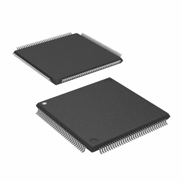
NXP Semiconductors MC9S12XDT512CAG — Microcontrollers & Processors (MCU / MPU / DSP)

NXP MC9S12XDT512CAG 16-bit MCU, 80MHz, 512KB Flash, 144-LQFP

MPNMC9S12XDT512CAG
End of Life

NXP HCS12X 16-bit MCU, MC9S12XDT512CAG, 80MHz core, 512KB Flash, 20K x 8 RAM, 4K x 8 EEPROM, 119 I/O, CAN/LIN/SPI/I2C/SCI, 24-ch 10-bit ADC, -40 to 85°C, 144-LQFP.

$42.33Ref. price · indicative, final on quote
Packaging144-LQFP
RoHSROHS3 Compliant
SeriesHCS12X
Independent supplier — new & surplus stockAuthenticity-screened · ESD-safe packingListing updated Aug 2026

Specifications

MC9S12XDT512CAG specifications
ParameterValue
SeriesHCS12X
MountingSurface Mount
Oscillator typeExternal
Program memory typeFLASH
Voltage - supply (Vcc (Vdd))2.35V ~ 5.5V
Operating temperature-40°C ~ 85°C (TA)
Speed80MHz
PackageTray
RAM size20K x 8
Core size16-Bit
EEPROM size4K x 8
PeripheralsLVD, POR, PWM, WDT
ConnectivityCANbus, EBI/EMI, I²C, IrDA, LINbus, SCI, SPI
Number of i (O)119
Core processorHCS12X
Case144-LQFP
Data convertersA/D 24x10b
Program memory size512KB (512K x 8)

Product details

16-bit HCS12X at 80 MHz — what the core speed buys you

It carries an on-chip 4 K x 8 EEPROM block for nonvolatile parameter storage, which saves a separate serial EEPROM on the BOM in many designs.

Memory architecture: Flash, RAM, and EEPROM allocation

The 512 KB Flash (512K x 8) is organized for code and constant data storage, while the 20 K x 8 RAM handles stack and variable space. The separate 4 K x 8 EEPROM block is rated for parameter storage that survives power cycles — think calibration coefficients, node IDs, or fault logs. Budget the EEPROM endurance for the expected write cycles over the product lifetime; the HCS12X family typically supports 100k write/erase cycles per byte, but confirm the exact specification in the datasheet for your retention temperature.

Connectivity and peripheral set for system integration

The 24-channel 10-bit ADC reduces the need for external multiplexers when monitoring multiple analog signals. On-chip peripherals include LVD (low-voltage detect), POR (power-on reset), PWM, and WDT — covering the basic supervisory and timing functions without external ICs.

Package and mounting: 144-LQFP (20x20 mm)

Housed in a 144-LQFP package with a 20x20 mm body, this MCU is a surface-mount device intended for standard reflow soldering. The 119 I/O pins fan out on a 0.5 mm pitch, which calls for careful PCB layout — route the high-speed CAN and SPI lines with controlled impedance if the trace length exceeds a few inches.

This is a standard-channel part available through NXP's distribution network.

Frequently asked questions

Does MC9S12XDT512CAG have built-in EEPROM?

Yes, the MC9S12XDT512CAG includes 4K x 8 of on-chip EEPROM for nonvolatile parameter storage, eliminating the need for an external serial EEPROM in many designs.

Can MC9S12XDT512CAG run at 80 MHz?

Yes, the core is rated for 80 MHz operation, which is the maximum clock speed for this HCS12X device. Ensure the PLL configuration and flash wait states are set correctly in firmware to avoid bus errors when raising the core clock.

What development tools support MC9S12XDT512CAG?

NXP provides the CodeWarrior for HCS12X IDE, along with hardware debug tools like the USB Multilink Universal and Tracelancer. Third-party tools from IAR and Cosmic also support the HCS12X architecture. The BDM (Background Debug Mode) interface on the 144-LQFP package gives access to the debug port for programming and in-circuit debugging.