20 MHz S08 core with LIN — a BOM-fit check for serial-bus slave nodes
The NXP MC9S08SE8CWL is an 8-bit MCU built around the S08 core, clocked at 20 MHz. On-chip peripherals include a 10-channel 10-bit ADC, LINbus and SCI serial interfaces, plus LVD, POR, and PWM.
Memory and speed — what fits, what doesn't
The 20 MHz clock is the headline performance rating for this 8-bit S08 core — it sets the timing budget for LIN/SCI communication and PWM update rates. The 8 KB Flash defines the firmware footprint ceiling: enough for a small LIN node or sensor hub, not for a multi-protocol gateway. The 512 bytes RAM constrains the buffer depth for SCI frames and ADC conversions — a key BOM-fit check against the application's data memory requirement.
Package and rework — 28-SOIC is a bench-friendly footprint
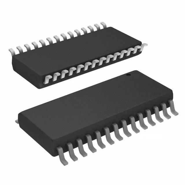
The 28-SOIC package (7.50 mm body) is a surface-mount footprint. The 0.295-inch width gives good pad access for hand-soldering or reflow touch-up.