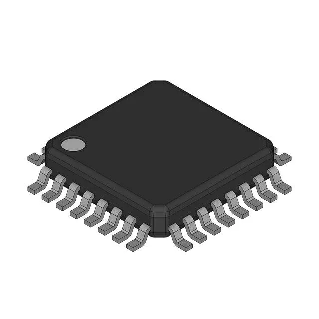
Core specs and BOM-fit for a control MCU
The MC9S08RG32CFJ is an NXP HCS08 8-bit microcontroller running at 8 MHz, with 32 KB of on-chip flash and 2 KB of RAM. That flash-to-RAM ratio (16:1) means the firmware image and lookup tables fit comfortably, but the data buffer space is tight — a control loop logging sensor values or holding a display frame needs to budget the 2 KB carefully. Its 25 general-purpose I/O pins in a 32-LQFP package give a solid pin-to-footprint ratio for simple control tasks like keypad scanning, LED driving, or relay toggling. On-chip peripherals include LVD (low-voltage detect) for brownout reset, POR for power-on reset, a PWM timer for dimming or motor speed control, and a watchdog timer for system supervision — all standard blocks that reduce external glue logic.
Serial connectivity and temperature grade
Serial communication is handled by one SCI (UART) module and one SPI module. The SCI supports asynchronous serial links to a host PC, Bluetooth module, or RS-485 transceiver; the SPI can talk to ADCs, DACs, or serial EEPROMs at bus speeds up to the core clock divided by 2. There is no I²C peripheral on this device — if your design needs I²C, you bit-bang it on two GPIOs or step up to the S08AC family. That covers unheated factory floors, outdoor enclosures in temperate climates, and engine bays with passive cooling. The 32-LQFP package measures 7x7 mm with a 0.8 mm pitch — fine enough for a two-layer board with careful fan-out, but the inner rows of the QFP may need a via to escape on a dense layout.
Lifecycle and compliance reality
One compliance caveat: the MC9S08RG32CFJ is listed as RoHS non-compliant. That likely means the plating or solder-ball alloy contains lead above the 0.1 % threshold. For markets with RoHS exemptions (military, aerospace, medical implant, some industrial controls) this is fine; for general EU consumer electronics it is a showstopper. Confirm the exemption status for your jurisdiction before committing the BOM line.