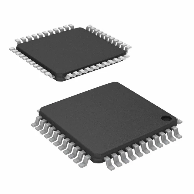
50 MHz 8-bit core in a 44-LQFP — what the bus speed means for a control loop
The MC9S08QE16CLD runs an 8-bit S08 core at 50 MHz, but the practical instruction throughput is gated by the flash access time — the 16 KB on-chip Flash (16K x 8) has zero-wait-state performance only up to about half the core clock; beyond that, the bus stalls for a cycle on each fetch. For a tight control loop polling an ADC and updating a PWM register, the effective MIPS lands closer to 25–30 MIPS unless the code fits entirely in the 1 KB RAM (1K x 8). The 10-channel 12-bit ADC (A/D 10x12b) samples at a rate limited by the conversion clock, not the core — budget 2–3 µs per conversion at the ADC's max clock. That is fast enough to oversample a 100 Hz sensor signal for noise averaging, but not for high-speed data acquisition above 200 kHz.
Memory budget — 16 KB Flash plus 1 KB RAM for a single-purpose controller
16 KB of program Flash (16K x 8) and 1 KB of RAM (1K x 8) set a hard ceiling on firmware complexity. A typical motor-control or sensor-interface application with a small RTOS or state machine fits — the HAL, peripheral drivers, and a modest application layer consume roughly 8–12 KB of Flash, leaving 4–8 KB for field-upgradeable firmware. The remaining RAM after stack and global variables is about 200–400 bytes for dynamic data. The internal oscillator (Oscillator Type: Internal) eliminates the external crystal for the core clock, saving two pins and the BOM cost of the resonator. The accuracy is typically ±2% over temperature — adequate for UART baud-rate generation at 115200 bps, but not for CAN or precision timing without calibration.
Peripheral set and serial connectivity for industrial buses
The MC9S08QE16CLD integrates I²C, LINbus, SCI (UART), and SPI (Connectivity: I²C, LINbus, SCI, SPI). The LINbus controller is a hardware LIN 2.0 node with automatic baud-rate detection — useful for automotive body-electronics subnets or industrial sensor networks that use LIN as a low-cost fieldbus. The SCI module supports full-duplex asynchronous serial up to 1.875 Mbps at 50 MHz core clock. 34 general-purpose I/O pins (Number of I/O: 34) are available in the 44-LQFP package. After allocating pins for the ADC channels (10), serial interfaces (up to 8 pins for I²C + SPI + SCI), and PWM outputs (up to 4 channels from the TPM module), roughly 12–16 GPIOs remain for discrete inputs, LED drivers, or keypad scanning.
Supply voltage and temperature grade for single-rail industrial designs
The low-voltage detect (LVD) peripheral (Peripherals: LVD, PWM, WDT) generates a reset or interrupt when the supply drops below a programmable threshold — essential for brownout protection in battery-powered or capacitor-backed applications. The 44-LQFP package (10x10 mm body, 0.8 mm pitch) is a standard quad flat pack — routable on a 2-layer PCB with 6/6 mil trace/space rules, though the inner rows of the 44-pin array may require a via to break out on a 2-layer board.
Sourced through independent distribution channels against an RFQ. The part is a standard catalog item for NXP; lead times typically run 8–12 weeks from the factory for volume orders, but spot quantities are available from distributor inventory.