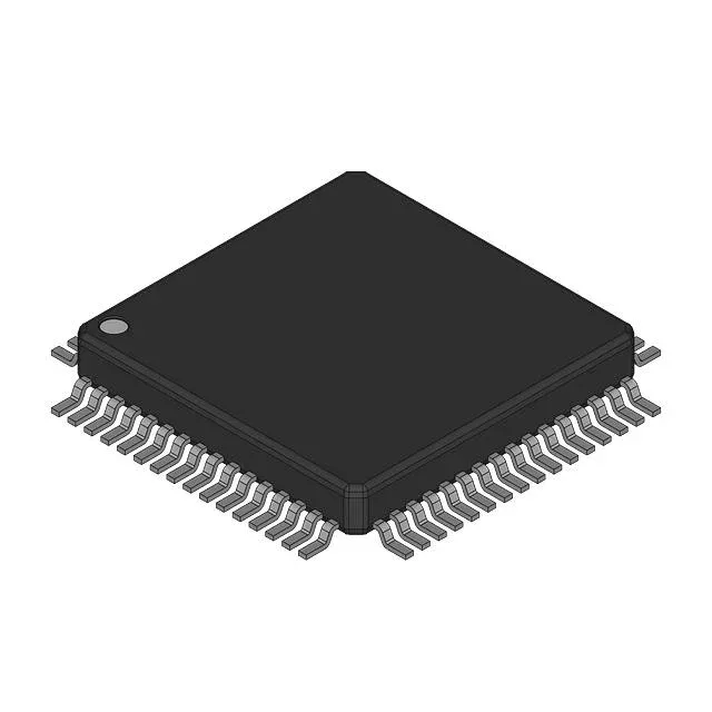
S08 core at 48 MHz with USB 2.0
The MC9S08JM32CQH: The headline peripheral is the USB 2.0 interface alongside I²C, SPI, SCI, and LINbus — this MCU handles both human-interface device (HID) class USB and sensor bus bridging on a single chip.
Peripheral mix and analog front-end
51 general-purpose I/O lines give the board designer room for a parallel LCD bus, keypad matrix, or multiple sensor interrupts without an external port expander. The 12-channel 12-bit ADC samples analog inputs at up to the core clock rate divided by the conversion clock prescaler — no external mux needed for a dozen thermistors or potentiometers. On-chip peripherals include a low-voltage detect (LVD) for brownout-safe shutdown, a power-on reset (POR) that eliminates the external reset supervisor, a PWM timer for motor or LED dimming, and a watchdog timer (WDT) for runaway-code recovery.
64-QFP footprint and board integration
Housed in a 64-QFP package with a 14x14 mm body (0.8 mm pitch typical for this class), the MC9S08JM32CQH mounts on standard surface-mount pads. The supplier device package is 64-QFP (14x14) — the same footprint as many NXP Kinetis K-series parts, so a board layout can accommodate either family with minor BOM changes. The external oscillator type means the clock source is a crystal or ceramic resonator off-chip — the designer selects the frequency and accuracy, not a factory-trimmed internal RC.