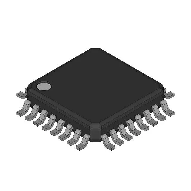
40MHz S08 core with 16KB Flash — what that means on the bench
The MC9S08DV16MLC is an 8-bit MCU from NXP's S08 family, clocked at 40 MHz with 16 KB of on-chip Flash program memory and 1 K x 8 of RAM. The 40 MHz speed sets the instruction throughput ceiling — for an 8-bit core, that's roughly 40 MIPS at peak, though real-world throughput depends on flash wait states and the instruction mix. The 16 KB Flash is enough for moderate control firmware with a CAN or LIN stack; the 1 KB RAM limits buffer-heavy applications like large data logging or multi-protocol gateways.
Peripherals and connectivity — CAN, LIN, SPI, I2C on one chip
The MC9S08DV16MLC integrates a CANbus controller, LINbus, SCI (UART), SPI, and I2C — all on a single 8-bit MCU. The 10-channel 12-bit ADC (A/D 10x12b) provides enough resolution for analog sensor inputs like temperature or pressure. Peripherals include LVD (low-voltage detect), POR (power-on reset), PWM, and WDT — the watchdog timer is essential for safety-critical firmware that must recover from hangs.
NXP lists the MC9S08DV16MLC as Active with no planned discontinuation. ROHS3 compliant — no exemptions that would require a transition to a different solder alloy. For a repair bench, that means the part is still a valid replacement for boards in the field; for a new design, it's safe to specify without worrying about a last-time-buy window.